AMBA AHB · Module 16
Memory Slave
Designing an AHB SRAM/memory slave — the same capture-then-act structure, but the storage is a large SRAM array (a compiled macro, not flops) and the new element is wait-state generation. When the memory isn't single-cycle (multi-cycle SRAM/flash, single-ported conflict, or registered read output), the slave drives HREADYOUT low until the memory is ready, then high; a fast single-cycle SRAM needs no waits. The bus interface to bulk storage, where memory timing becomes bus timing.
Chapters 16.1 and 16.2 built slaves whose storage was a handful of registers, then a parameterised register array — and both were zero-wait: they responded in a single cycle, so HREADYOUT stayed high. This chapter builds a memory slave — an AHB-Lite slave backed by a large SRAM array rather than registers — and with it introduces the first slave that cannot always answer in one cycle. The structure is still the same capture-then-act backbone (16.1): capture the address-phase context (sel_q, write_q, addr_q), then act in the data phase. The storage changes — a parameterised SRAM (often a compiled macro) instead of flops — and the access changes accordingly (drive addr/wdata/we into the SRAM on a write; drive addr and return rdata on a read). But the genuinely new element is wait-state generation: real memories are sometimes not single-cycle — a multi-cycle SRAM/flash needs several cycles, a single-ported SRAM shared with another path can conflict, a registered read output adds a cycle of latency. When the memory isn't ready, the slave drives HREADYOUT low (insert wait states — chapter 6.2), holding the master, then drives it high when the data is available. (A fast single-cycle SRAM needs no wait states — HREADYOUT stays high, exactly like the simple slave.) This chapter builds the memory slave and its wait-state logic — the slave side of slave-inserted wait states.
1. What Is It?
A memory slave is an AHB-Lite slave whose storage is a large SRAM/memory array (not individual registers), with wait-state generation for when the memory isn't single-cycle. Its parts:
- Same capture-then-act — capture the address-phase context (
sel_q,write_q,addr_q), act in the data phase (16.1's structure). - SRAM array — the storage is a parameterised memory (a compiled SRAM macro or inferred array), not flops; accessed by
addr,wdata,we, returningrdata. - Wait-state generation — when the memory isn't ready (multi-cycle, single-ported conflict, registered read), drive
HREADYOUTlow; drive it high when the data is available. - Zero-wait when fast — a single-cycle SRAM needs no wait states (
HREADYOUTstays high, like the simple slave).
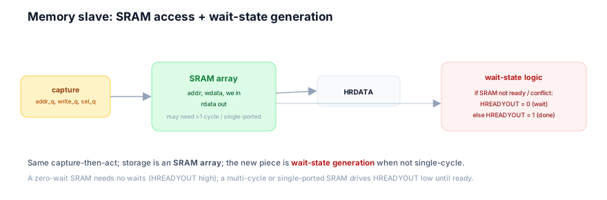
So a memory slave is the simple slave (16.1) with SRAM storage and wait-state generation: the structure (capture-then-act, qualified select, registered context) is identical, but the storage becomes a large SRAM array (a compiled macro, not flops — because thousands/millions of locations can't be flops), and — crucially — the slave gains the ability to insert wait states when the memory can't answer in one cycle. The write path drives the SRAM's addr/wdata/we; the read path drives addr and muxes rdata onto HRDATA. The wait-state logic drives HREADYOUT low while the memory is busy and high when it's ready. It is the first slave whose timing is non-trivial.
2. Why Does It Exist?
The memory slave exists because systems need bulk storage (RAM, ROM, flash) on the bus — far more than registers can hold — and that storage is backed by memory arrays that aren't always single-cycle, so the slave must be able to insert wait states to match the memory's real timing.
The bulk storage need is the root: a system needs memory — instruction/data RAM, ROM/flash for code, framebuffers, scratchpads — often kilobytes to megabytes. That's far more than a register bank (dozens of registers) can hold, and it can't be built from individual flops (a megabyte of flops is absurd in area). So bulk storage uses dense memory arrays — SRAM (compiled macros), flash, DRAM — and those need a slave to put them on the bus. The memory slave exists to expose bulk memory over AHB.
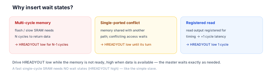
The memory isn't always single-cycle drives the wait states: dense memories aren't always able to respond in one cycle. A small, fast SRAM might be single-cycle. But a larger or slower SRAM, a flash (slow), a single-ported SRAM shared between two access paths (one must wait), or a memory with a registered read output (pipelined for timing) needs more than one cycle — or needs to stall a conflicting access. The bus, though, expects a response — and AHB's mechanism for "not ready yet" is wait states (HREADYOUT low — chapter 6.2). So the memory slave must generate wait states to match the memory's real timing — holding the master while the memory works, then completing. Wait-state generation exists because memories are not always single-cycle.
The bus-timing decoupling is the deeper why: wait states decouple the bus protocol (which is fixed) from the memory's timing (which varies by memory type/speed). The master doesn't need to know how fast the memory is — it just waits when HREADYOUT is low and proceeds when it's high. So the same master works with a fast SRAM (zero waits) or a slow flash (many waits) — the slave absorbs the difference by inserting the right number of waits. So wait states are how the bus adapts to any memory speed without changing the master. Wait-state generation is the adaptation layer between the fixed bus and the variable memory. In summary, the memory slave exists because: systems need bulk storage (RAM/ROM/flash — far beyond registers, backed by dense memory arrays, not flops — the why); those memories aren't always single-cycle (multi-cycle, single-ported conflict, registered read — driving wait-state generation); and wait states decouple the fixed bus from the variable memory timing (the same master works with any memory speed — the adaptation). So the memory slave is the bus interface to bulk memory, and its wait-state generation is what lets a fixed bus protocol serve memories of any speed — the slave absorbing the timing difference. This chapter builds the first slave that manages bus timing.
3. Mental Model
Model the memory slave as a librarian at a counter (the bus interface) backed by a vast archive (the SRAM). For a book on the front shelf, the librarian hands it over instantly (zero wait — HREADYOUT high). But for a book in deep storage — or when someone else is already at the only retrieval cart (single-ported conflict) — the librarian says "one moment" and holds up a wait sign (HREADYOUT low) until the book arrives, then hands it over (HREADYOUT high).
A librarian at a counter (the bus interface) backed by a vast archive (the SRAM array — far bigger than a desk of forms, which was the register bank). You hand the librarian a call number (the captured address) and either a book to file (a write) or a request to fetch (a read). For a book on the front shelf — a fast, single-cycle SRAM — the librarian files it or hands it over instantly: no waiting, the counter is immediately free for the next person (HREADYOUT stays high — zero wait, exactly like the register desk). But the archive is vast, and not every book is on the front shelf. A book in deep storage — a multi-cycle memory — takes several minutes to retrieve: the librarian says "one moment" and holds up a wait sign (HREADYOUT low), making you wait at the counter, then hands it over when it arrives (HREADYOUT high). Or the archive has only one retrieval cart (a single-ported SRAM) and someone else is already using it (a conflicting access) — again the librarian holds up the wait sign until the cart is free, then serves you. Or the librarian double-checks every book at a side desk before handing it over (a registered read output) — adding one fixed extra moment each time. In every case, the wait sign (HREADYOUT low) means "not ready — hold on", and taking it down (HREADYOUT high) means "here it is — done". You, at the counter, just wait when the sign is up — you don't need to know why it's slow. So the librarian absorbs the archive's slowness by holding you at the counter exactly as long as needed.
This captures the memory slave: the librarian at the counter = the bus interface (capture-then-act); the vast archive = the SRAM array; the call number = the captured address (addr_q); front-shelf instant service = a fast single-cycle SRAM (HREADYOUT stays high, zero wait); deep-storage "one moment" with the wait sign up = a multi-cycle memory (HREADYOUT low for the wait cycles); the single retrieval cart in use = a single-ported SRAM conflict (wait until free); double-checking at the side desk = a registered read output (+1 cycle latency); taking the wait sign down = HREADYOUT high (data ready, transfer completes); you just waiting without knowing why = the master simply holding while HREADYOUT is low. The slave absorbs the memory's slowness by holding the bus exactly as long as needed.
Watch a zero-wait write followed by a read that needs one wait state:
Zero-wait write, then a read with one wait state
5 cyclesThe model's lesson: the slave absorbs the memory's slowness by holding the bus exactly as long as needed. In the waveform, the single-cycle write completes with HREADYOUT high (zero wait), while the multi-cycle read drives HREADYOUT low for one wait cycle — holding the master — then high with the data valid.
4. Real Hardware Perspective
In hardware, the memory slave is a compiled SRAM macro (or inferred array), an address/write-data/write-enable path into it, a read-data mux onto HRDATA, and wait-state logic driving HREADYOUT — the timing of which depends on the SRAM's latency.
The SRAM macro: bulk storage isn't flops — it's a compiled SRAM macro (a dense, custom-laid-out memory block from a memory compiler) or, for small/FPGA memories, an inferred array (reg [W-1:0] mem [0:DEPTH-1]) that the tool maps to block RAM. The macro has ports: an addr, a wdata, a write-enable (we), and a rdata output. So in hardware, the storage is a memory macro with those ports. The slave drives those ports from the AHB context.
The access path: on a write (sel_q && write_q in the data phase), the slave drives the SRAM's addr = addr_q, wdata = HWDATA, we = 1 — writing HWDATA to location addr_q. On a read (sel_q && !write_q), it drives addr = addr_q, we = 0, and the SRAM's rdata is muxed onto HRDATA. (A subtlety: SRAMs are usually synchronous — addr is presented one cycle, rdata comes the next — which itself can mean a registered-read latency to manage. The address-phase/data-phase pipelining of AHB aligns well here: the address is available in the address phase, so a synchronous SRAM read launched then can have rdata ready in the data phase.) The access path therefore drives the SRAM ports and muxes rdata onto HRDATA — though which address it drives differs between reads and writes, as the RTL below shows.
The wait-state logic: this is the new piece. HREADYOUT reflects whether the memory is ready. For a single-cycle SRAM (read launched in the address phase, rdata ready in the data phase), HREADYOUT stays high — zero wait. For a multi-cycle memory, the slave needs a small counter/FSM: when an access starts, drive HREADYOUT low and count the memory's latency; when the count expires (data ready), drive HREADYOUT high and complete. For a single-ported SRAM with a conflict (e.g. a second access path also using the SRAM), the slave drives HREADYOUT low until the conflict clears (its turn comes). For a registered read output, there's a fixed one-cycle stall on reads. So in hardware, the wait-state logic is a counter/FSM (or simple combinational condition) that drives HREADYOUT low while the memory is busy, high when ready. Crucially, HREADYOUT must follow the wait-state rules (chapter 6.2): once a wait is being inserted, the slave holds HREADYOUT low for the needed cycles and the control/data stay stable; the master is held automatically. So in hardware, the memory slave is a compiled SRAM macro + an access path (drive addr/wdata/we, mux rdata) + wait-state logic (a counter/FSM driving HREADYOUT to match the memory's latency). The timing details (synchronous SRAM, registered reads) make this the first slave where getting the cycle-by-cycle HREADYOUT timing right is the core challenge. The timing is the hard part.
5. System Architecture Perspective
At the system level, the memory slave is the bus interface to bulk storage, and its wait-state generation is the mechanism that lets a single, fixed bus serve memories of wildly different speeds — from fast on-chip SRAM to slow flash — without the master ever knowing the difference.
The bulk-storage interface: the memory slave is how the system's bulk memory (instruction/data RAM, ROM, flash, scratchpads) sits on the bus. The CPU fetches code from a ROM/flash memory slave, reads/writes data in a RAM memory slave, accesses framebuffers and scratchpads — all through memory slaves. Memory slaves are therefore the storage tier on the bus — the largest and most-accessed slaves in the system.
The speed-adaptation via wait states: different memories have wildly different speeds — a tightly-coupled SRAM might be single-cycle, an on-chip flash might need many cycles, an external memory (through a controller) many more. Yet they all connect to the same bus with the same protocol. The wait-state mechanism is what makes this work: each memory slave inserts as many waits as its memory needs — zero for fast SRAM, several for flash, many for external — and the master simply waits (HREADYOUT low) without knowing or caring why. So at the system level, wait states adapt the one bus to many memory speeds — the slave absorbs the speed difference. Wait states are the speed-adaptation layer that lets memories of any speed coexist on one bus.
The performance consequence: because memory slaves can insert waits, memory speed directly affects system performance (chapter 14.4 — the wait-state penalty). A slow memory (many waits) stalls the CPU on every access — a bottleneck (chapter 14.8). So system architects care about memory slave timing: they put hot code/data in fast (zero/low-wait) memory, use caches to hide slow-memory latency, and budget the wait states. So the memory slave's wait-state behavior is a first-order performance factor — not just a correctness detail. So at the system level, the memory slave is the bus interface to bulk storage (the storage tier — RAM/ROM/flash, the most-accessed slaves), its wait-state generation adapts the fixed bus to any memory speed (the slave absorbing the difference — fast SRAM to slow flash, transparently to the master), and its timing is a first-order performance factor (the wait-state penalty — chapter 14.4 — driving memory hierarchy, caching, and placement decisions). The memory slave is where storage meets the bus, and where memory speed becomes bus timing.
6. Engineering Tradeoffs
The memory slave embodies the SRAM-backed, wait-state-generating, timing-matched design.
- SRAM macro vs flops. A compiled SRAM macro is dense (the only feasible way to build bulk memory) at the cost of fixed ports and timing; flops are flexible but absurd in area beyond a few registers. Use a macro for bulk storage.
- Zero-wait vs multi-cycle memory. A fast single-cycle SRAM gives zero-wait access (best performance) but may be small/costly; a slower/larger/cheaper memory needs wait states (lower performance). Trade speed for capacity/cost; place hot data in fast memory.
- Single-ported vs dual-ported SRAM. A single-ported SRAM is smaller/cheaper but forces conflicting accesses to wait (wait states on conflict); a dual-ported SRAM avoids the conflict at higher area. Choose by access pattern.
- Registered read output vs combinational. Registering the read output helps timing closure (higher clock) at the cost of +1 cycle read latency (a wait state); a combinational read avoids the latency but may limit frequency. Trade frequency for latency.
The throughline: a memory slave is the simple slave (16.1) backed by a large SRAM array (a compiled macro, not flops) instead of registers — the same capture-then-act structure (capture sel_q, write_q, addr_q; act in the data phase), driving the SRAM's addr/wdata/we on a write and muxing rdata to HRDATA on a read. The new element is wait-state generation: when the memory isn't single-cycle (multi-cycle SRAM/flash, single-ported conflict, or registered read output), the slave drives HREADYOUT low (inserting wait states — chapter 6.2) until the memory is ready, then high. A fast single-cycle SRAM needs no waits (HREADYOUT stays high). It's the bus interface to bulk storage, and its wait-state timing is a first-order performance factor (the wait-state penalty — chapter 14.4).
7. Industry Example
Build a memory slave for an on-chip instruction SRAM, then contrast with a flash.
A CPU fetches instructions from an on-chip SRAM (fast) and from on-chip flash (slow) — both memory slaves on the bus.
- The SRAM (single-cycle, zero wait). The instruction SRAM is a fast, single-ported, synchronous SRAM. The slave captures
addr_qin the address phase and launches the SRAM read then; the synchronous SRAM presentsrdatain the next cycle — which is the AHB data phase. Sordatais ready in the data phase,HREADYOUTstays high, and the read completes zero-wait. The address-phase/data-phase pipelining of AHB aligns perfectly with the synchronous SRAM's one-cycle read latency. So a well-matched SRAM gives zero-wait access — the best case. - The flash (multi-cycle, several waits). The on-chip flash is slow — say it needs 4 cycles to return data. The flash memory slave, on a read, drives
HREADYOUTlow and starts a 4-cycle counter; for cycles 1-3 it holdsHREADYOUTlow (3 wait states), keeping the master waiting and the access in progress; in cycle 4, when the flash data is ready, it muxesrdataontoHRDATAand drivesHREADYOUThigh — completing the read. So every flash fetch costs 4 cycles (3 waits) — slow, but correct. - The performance contrast. Fetching from SRAM is zero-wait (1 cycle/access); fetching from flash is 4 cycles/access. So code in SRAM runs 4× faster (per fetch) than code in flash. This is exactly why systems copy hot code from flash to SRAM at boot, or use an instruction cache to hide flash latency — the wait-state penalty (chapter 14.4) of the flash is a real performance cost the architecture works around.
- Single-ported conflict (if shared). If the SRAM were shared (e.g. CPU instruction fetch and a DMA both accessing it through one port), a conflict would force one to wait — the slave drives
HREADYOUTlow on the loser until the port is free. (A dual-ported SRAM would avoid this, at higher area.)
The example shows the memory slave across the speed spectrum: a fast SRAM (zero-wait, AHB pipelining aligned with the synchronous read), a slow flash (multi-cycle, several wait states via a counter), the performance contrast (driving SRAM-copy/caching decisions), and the single-ported conflict (waits on contention). The same slave structure (capture-then-act + SRAM access) serves both, differing only in the wait-state timing matched to each memory.
7b. The Memory Slave, Written Out
The prose above contains one structural claim worth making concrete: a synchronous SRAM read launched in the address phase returns its data in the data phase, so a well-matched SRAM is zero-wait. That single sentence decides the whole design, because it means reads and writes use different addresses.
- A read must present
HADDR— the unregistered, address-phase value — to the SRAM, so the SRAM's own output register producesrdataduring the data phase. - A write must present
addr_q— the registered value — because the data it writes,HWDATA, only arrives in the data phase.
Register the address for reads as well and the read costs an extra cycle for no reason. That asymmetry is the subject of the Debug Lab below.
module ahb_sram_slave #(
  parameter int AW    = 32,
  parameter int DW    = 32,
  parameter int DEPTH = 4096            // words
) (
  input  logic          HCLK,
  input  logic          HRESETn,
  input  logic          HSEL,
  input  logic [1:0]    HTRANS,
  input  logic [AW-1:0] HADDR,
  input  logic          HWRITE,
  input  logic [2:0]    HSIZE,
  input  logic          HREADY,        // GLOBAL ready from the interconnect
  input  logic [DW-1:0] HWDATA,
  output logic          HREADYOUT,
  output logic [DW-1:0] HRDATA,
  output logic [1:0]    HRESP
);
  localparam int LSB  = $clog2(DW/8);          // byte-offset bits
  localparam int IDXW = $clog2(DEPTH);
  localparam logic [1:0] RSP_OKAY = 2'b00;

  // ── Address phase ───────────────────────────────────────────────────────
  // HTRANS[1] is set for NONSEQ and SEQ, clear for IDLE and BUSY.
  wire            ap_valid   = HSEL && HTRANS[1];
  wire            ap_read    = ap_valid && !HWRITE;
  wire [IDXW-1:0] ap_idx     = HADDR[LSB +: IDXW];

  // ── Registered context for the data phase ───────────────────────────────
  // Accept a new address phase only when the bus is advancing AND this slave
  // is releasing. Using HREADY alone would re-capture during our own stall.
  wire capture_en = HREADY && HREADYOUT;

  logic            dp_sel, dp_write;
  logic [IDXW-1:0] dp_idx;

  always_ff @(posedge HCLK or negedge HRESETn) begin
    if (!HRESETn) begin
      dp_sel <= 1'b0; dp_write <= 1'b0; dp_idx <= '0;
    end else if (capture_en) begin
      dp_sel <= ap_valid; dp_write <= ap_valid && HWRITE; dp_idx <= ap_idx;
    end
  end

  // ── The single SRAM port, and the one place it is contended ─────────────
  // A data-phase write and the next transfer's address-phase read launch land
  // in the SAME cycle, because AHB overlaps them. One port cannot serve both.
  wire dp_write_active = dp_sel && dp_write;

  logic wr_done;          // this transfer's write has already been issued
  wire  do_write = dp_write_active && !wr_done;

  // NOTE: ap_read here is deliberately NOT qualified by HREADY. Qualifying it
  // would make HREADYOUT depend on HREADY, and the interconnect derives HREADY
  // from HREADYOUT - a combinational loop. The master holds its address phase
  // while stalled, so the unqualified form is stable and safe.
  wire port_conflict = do_write && ap_read;

  // Give the port to the write and stall one cycle; the read launches next.
  assign HREADYOUT = !port_conflict;

  always_ff @(posedge HCLK or negedge HRESETn)
    if (!HRESETn)         wr_done <= 1'b0;
    else if (capture_en)  wr_done <= 1'b0;   // new transfer: re-arm
    else if (do_write)    wr_done <= 1'b1;   // stalled after writing

  // ── SRAM ────────────────────────────────────────────────────────────────
  // Reads present the ADDRESS-PHASE index; writes present the REGISTERED one.
  logic [DW-1:0]   mem [DEPTH];
  logic [DW-1:0]   sram_q;
  wire [IDXW-1:0]  sram_idx = do_write ? dp_idx : ap_idx;

  always_ff @(posedge HCLK) begin
    if (do_write) mem[sram_idx] <= HWDATA;
    // The output register is what aligns a read launched in the address phase
    // with the data phase. It is the SRAM's latency, not an extra stage.
    sram_q <= mem[sram_idx];
  end

  assign HRDATA    = sram_q;
  assign HRESP     = RSP_OKAY;   // see /protocols/ahb/error-response for faults

  // ── Alignment. AMBA requires every transfer to be aligned to its HSIZE.
  //    An unaligned access silently indexes the wrong word rather than failing
  //    visibly, so it is worth asserting.
  // synthesis translate_off
  always_ff @(posedge HCLK)
    if (HRESETn && capture_en && ap_valid)
      assert ((HADDR & ((1 << HSIZE) - 1)) == '0)
        else $error("unaligned AHB access: HADDR=%h HSIZE=%0d", HADDR, HSIZE);
  // synthesis translate_on
endmodule
Two design notes that the structure makes visible.
Reads are zero-wait; a write immediately followed by a read costs one cycle. That is not a defect, it is the cost of one SRAM port. A dual-port SRAM removes it. So does a one-entry write buffer that defers the write until the port is idle — at the price of a read-after-write hazard, since a read of an address still sitting in the buffer must be forwarded rather than fetched. The stall version has no such hazard, which is why it is the right starting point.
HREADYOUT must not depend combinationally on HREADY. The interconnect
builds HREADY from the selected slave's HREADYOUT, so a slave that qualifies
its stall condition with HREADY closes a combinational loop. The comment in the
RTL marks the one place this matters.
Proving it
module ahb_sram_slave_tb;
  localparam int AW = 32, DW = 32;

  logic HCLK = 0, HRESETn = 0;
  logic HSEL = 0, HWRITE = 0;
  logic [1:0] HTRANS = 2'b00;
  logic [AW-1:0] HADDR = '0;
  logic [2:0] HSIZE = 3'b010;
  logic [DW-1:0] HWDATA = '0;
  logic HREADYOUT; logic [DW-1:0] HRDATA; logic [1:0] HRESP;

  // Single-slave interconnect: HREADY is this slave's HREADYOUT.
  wire HREADY = HREADYOUT;

  ahb_sram_slave #(.AW(AW), .DW(DW), .DEPTH(256)) dut (.*);

  always #5 HCLK = ~HCLK;
  int fails = 0;

  // Drive one address phase, then hold it until the bus accepts it.
  task automatic addr_phase (input bit wr, input logic [AW-1:0] a);
    @(negedge HCLK);
    HSEL = 1; HTRANS = 2'b10; HWRITE = wr; HADDR = a;
    @(posedge HCLK);
    while (!HREADY) @(posedge HCLK);       // held while the slave stalls
  endtask

  task automatic idle_phase ();
    @(negedge HCLK); HSEL = 0; HTRANS = 2'b00;
  endtask

  task automatic chk (input string what, input logic [DW-1:0] got, exp);
    if (got !== exp) begin
      $error("%s: got %h expected %h", what, got, exp); fails++;
    end else $display("PASS %-32s = %h", what, got);
  endtask

  initial begin
    repeat (2) @(negedge HCLK); HRESETn = 1;

    // --- Write 0xA5A5_0001 to word 4 -------------------------------------
    addr_phase(1'b1, 32'h0000_0010);
    @(negedge HCLK) HWDATA = 32'hA5A5_0001;   // data phase
    idle_phase();
    @(posedge HCLK);

    // --- Read it back. Reads are zero-wait: the launch happens in the
    //     address phase, so HRDATA is valid in the very next cycle.
    addr_phase(1'b0, 32'h0000_0010);
    idle_phase();
    @(posedge HCLK);                          // data phase
    chk("read-back of word 4", HRDATA, 32'hA5A5_0001);

    // --- Back-to-back write then read: the port conflict.
    //     The slave must stall exactly ONE cycle, and the read must still
    //     return the value the write just committed.
    addr_phase(1'b1, 32'h0000_0020);
    begin
      int stalls = 0;
      @(negedge HCLK) HWDATA = 32'hDEAD_BEEF;
      // Present the read's address phase in the write's data phase - this is
      // the cycle where both want the SRAM port.
      HSEL = 1; HTRANS = 2'b10; HWRITE = 0; HADDR = 32'h0000_0020;
      @(posedge HCLK);
      while (!HREADY) begin stalls++; @(posedge HCLK); end
      chk("write->read stalls exactly 1 cycle", stalls[3:0], 4'd1);
      idle_phase();
      @(posedge HCLK);
      chk("read after write sees new data", HRDATA, 32'hDEAD_BEEF);
    end

    if (fails == 0) $display("All memory-slave checks passed.");
    else            $fatal(1, "%0d check(s) failed", fails);
    $finish;
  end
endmodule
The third check is the one worth keeping. It asserts the stall is exactly one cycle — not "at least one", which would pass a slave that stalls forever, and not "zero", which would pass a slave that silently drops the write.
Every read cost an extra cycle and nobody could find the wait state
REGISTERED-READ-ADDRESSAn instruction SRAM slave worked correctly but ran at roughly half the expected fetch rate. Every read took two data-phase cycles instead of one, on every access, with no pattern related to address or burst type. The SRAM vendor's datasheet specified a single-cycle synchronous read, and the timing report showed plenty of slack, so the memory was not the constraint.
Profiling put the CPU at about 55% of its projected throughput on code running from this SRAM, and at full rate on code running from a different slave.
// The read presented the REGISTERED address to the SRAM.
wire [IDXW-1:0] sram_idx = dp_idx;              // <-- always registered

always_ff @(posedge HCLK) begin
  if (do_write) mem[sram_idx] <= HWDATA;
  sram_q <= mem[sram_idx];
end

// ...which meant rdata arrived a cycle late, so the slave had to stall:
assign HREADYOUT = !(dp_sel && !dp_write && !read_launched);Lining up the address against the SRAM's input showed it immediately:
  cycle          1        2        3        4
  HADDR          A        -        B        -
  HTRANS       NONSEQ   IDLE    NONSEQ    IDLE
  addr_q         -        A        -        B     <- registered, one cycle late
  sram_idx       -        A        -        B     <- SRAM sees A in cycle 2
  sram_q         -        -        A        -     <- data arrives in cycle 3
  HREADYOUT      1        0        1        0     <- forced stall every read
The SRAM received address A in cycle 2 and produced its data in cycle 3 — but
cycle 2 was the data phase, so the slave had already missed its window and had
to stall. The address had been available on HADDR throughout cycle 1, one full
cycle earlier than it was used.
The design applied the capture-then-act rule uniformly, and it does not apply
uniformly. Capture exists so the data phase can act on the transfer's context
after the address phase has moved on — which a write genuinely needs, because
HWDATA only arrives in the data phase. A read needs the opposite: the SRAM has
its own output register, so presenting the address one cycle earlier is exactly
what makes the data land in the data phase.
Registering the address adds a second register in series with the SRAM's internal one. Two registers, two cycles of latency, and the slave then had to insert a wait state to cover the cycle it had spent on its own pipeline stage. The wait state was not the bug; it was the design correctly compensating for a bug one level up, which is why looking at the wait-state logic never found anything wrong with it.
The reason the SRAM datasheet was misleading here is that it was accurate. The memory really was single-cycle. The slave had added a cycle in front of it.
// Reads present the ADDRESS-PHASE index; only writes need the registered one.
wire [IDXW-1:0] sram_idx = do_write ? dp_idx : ap_idx;
One line, and reads become zero-wait. The testbench check that proves it is the
read-back above: with the fixed RTL HRDATA is valid in the first data-phase
cycle, and the while (!HREADY) loop in addr_phase never iterates.
Verifying it properly means measuring the stall count rather than only the data, because a slave that returns correct data slowly passes every value check ever written. The assertion worth binding is a latency bound rather than a value:
// A read to this zero-wait memory must complete in its first data-phase cycle.
a_read_zero_wait: assert property (@(posedge HCLK) disable iff (!HRESETn)
  (HREADY && HSEL && HTRANS[1] && !HWRITE) |=> HREADYOUT)
  else $error("read inserted an unexpected wait state");
The general lesson is worth more than the fix: capture-then-act is a rule about context, not about addresses. Register what the data phase cannot otherwise know — the direction, the selection, the address for a write. Do not register what a downstream pipeline stage is going to register for you. For the wait-state rules this slave has to honour see slave-inserted wait states, and for the capture discipline itself see address / control capture.
8. Common Mistakes
9. Interview Insight
Memory slave design is a practical RTL interview topic — the SRAM-vs-flops point, the wait-state generation, and the HREADYOUT-timing discipline are the signals.
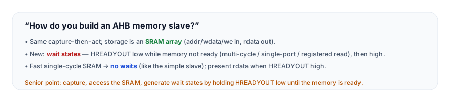
The answer that lands gives the structure and the wait-state timing: "A memory slave is the simple slave backed by a large SRAM array instead of registers. It keeps the same capture-then-act structure — capture the qualified select, the write flag, and the address in the address phase, then act in the data phase — but the storage is a compiled SRAM macro, not flops, because you can't build kilobytes or megabytes from individual registers. On a write, it drives the SRAM's address, write data, and write enable; on a read, it drives the address and muxes the SRAM's read data onto HRDATA. The genuinely new element compared to a register slave is wait-state generation. Real memories aren't always single-cycle. A fast SRAM might be, and there AHB's address-phase/data-phase pipelining aligns nicely with a synchronous SRAM — you launch the read in the address phase and the data's ready in the data phase, so HREADYOUT stays high, zero-wait. But a multi-cycle memory like flash, or a single-ported SRAM with a conflicting access, or a registered read output, can't answer in one cycle. In those cases the slave drives HREADYOUT low to insert wait states, holding the master, then drives it high when the data is actually ready. The critical discipline is the HREADYOUT timing: you drive it low for exactly the memory's latency — if you drive it high before the data's ready, the master samples garbage, a data-corruption bug; during the wait you hold the captured address and the access stable; and you present valid HRDATA in the cycle HREADYOUT goes high. That's usually a small FSM or counter that models the memory's latency. And the wait states matter for performance — a slow memory stalls the CPU on every access, which is why systems put hot code in fast SRAM or use caches." The SRAM-vs-flops point, the wait-state generation, and the precise HREADYOUT-timing discipline are the senior signals.
10. Practice Challenge
Build and reason from the memory slave.
- The structure. Describe the memory slave: SRAM array storage (not flops), capture-then-act access (drive
addr/wdata/we, muxrdata). - Wait-state sources. List the reasons a memory slave inserts wait states (multi-cycle, single-ported conflict, registered read) and what
HREADYOUTdoes in each. - Read the waveform. From Figure 2, explain the zero-wait write and the one-wait-state read (what
HREADYOUTdoes and whenHRDATAis valid). - HREADYOUT timing. Explain why driving
HREADYOUThigh too early corrupts data and too late wastes cycles — and what must stay stable during the wait. - Synchronous SRAM. Explain how AHB's address-phase/data-phase pipelining lets a fast synchronous SRAM be zero-wait, and when you still need waits.
11. Key Takeaways
- A memory slave is the simple slave backed by a large SRAM array (a compiled macro, not flops) instead of registers — same capture-then-act, driving the SRAM's
addr/wdata/weon a write and muxingrdatatoHRDATAon a read. - The new element is wait-state generation — real memories aren't always single-cycle (multi-cycle SRAM/flash, single-ported conflict, registered read), so the slave drives
HREADYOUTlow until the memory is ready, then high (chapter 6.2). - A fast single-cycle SRAM needs no wait states —
HREADYOUTstays high; AHB's address-phase/data-phase pipelining aligns with a synchronous SRAM's one-cycle read for zero-wait access. - HREADYOUT timing must be exact — drive it high in the cycle the data is valid: too early → the master samples garbage (corruption); too late → wasted cycles. Usually a small FSM/counter models the memory latency.
- Hold during the wait — while
HREADYOUTis low, the capturedaddr_q/write data and the access must stay stable (else wrong location);HRDATAneed only be valid whenHREADYOUTis high. - It's the bus interface to bulk storage — the storage tier (RAM/ROM/flash), and its wait-state timing is a first-order performance factor (the wait-state penalty — chapter 14.4 — driving caching/placement).
11b. Where This Is Specified
- Arm AMBA 5 AHB Protocol Specification (ARM IHI 0033). The address-phase/data-phase pipeline that overlaps transfer N's data phase with transfer N+1's address phase; the requirement that a manager holds its address phase stable while
HREADYis low; the rule that transfers are aligned to the size given byHSIZE; and the distinction between a subordinate'sHREADYOUTand the interconnect's combinedHREADY. - Arm AMBA 3 AHB-Lite Protocol Specification (ARM IHI 0033A). Slave-inserted wait states and the
HREADYOUTcontract for the single-manager subset. - IEEE 1800-2023 §6.9 and §27 — unpacked array declarations for the memory model, and the elaboration rules for parameterised depth.
- IEEE 1800-2023 §16 — the concurrent assertion used for the zero-wait read latency bound and the alignment check.
12. What Comes Next
You now can build a memory slave with wait-state generation. The next chapters drill into the slave's output-generation logic in detail:
- HREADYOUT Generation (next) — implement correct per-slave
HREADYOUTtiming in full. - HRDATA Muxing, HRESP Generation, and the rest — the richer slave RTL output paths.
To revisit the simple slave this extends, see A Simple AHB-Lite Slave; for the wait-state mechanism itself, see Slave-Inserted Wait States and What HREADY Means.