AMBA AHB · Module 16
Register Bank Slave
Extending the simple AHB-Lite slave into a parameterised register bank — the same capture-then-act structure, but the registers are an indexed array (by addr_q): a write decoder selects which register receives HWDATA (if writable), a read mux selects the indexed register onto HRDATA. Each register has access attributes (RW / RO / write-1-to-clear / read-to-clear / reserved-reads-0). Read-to-clear especially needs the qualified select. The workhorse peripheral interface, typically generated from a register map.
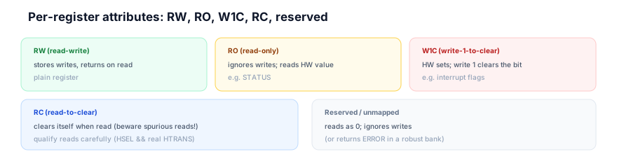
Chapter 16.1 built a slave with a few fixed registers; this chapter generalizes it into a parameterised register bank — a configurable array of registers, the workhorse interface of nearly every peripheral. The structure keeps the same capture-then-act backbone (16.1): capture the address-phase context (sel_q, write_q, the register index from addr_q), then act in the data phase. But now the registers are an indexed array: a write decoder uses the index to select which register receives HWDATA (and only registers that are writable accept it), and a read mux uses the index to select the addressed register onto HRDATA. The key new dimension is per-register access attributes: registers aren't all plain read-write — some are read-only (RO, e.g. STATUS — ignore writes), some have write-one-to-clear (W1C, e.g. interrupt flags — hardware sets, software clears by writing 1), some are read-to-clear (RC — clears on read), and reserved indices read as 0 (and ignore writes). The bank is parameterised by register count and width. A subtle point: read-to-clear registers especially need the qualified select (chapter 16.1) — so an idle cycle doesn't spuriously clear them. This chapter builds the parameterised register bank with its per-register access rules.
1. What Is It?
A register bank slave is a parameterised AHB-Lite slave whose storage is an indexed array of registers with per-register access attributes. Its parts:
- Same capture-then-act — capture the address-phase context (
sel_q,write_q, the register index fromaddr_q), act in the data phase (16.1's structure). - Indexed array — the registers are a parameterised array (count, width); the index selects one.
- Write decoder — the index selects which register receives
HWDATA(only writable registers accept it). - Read mux — the index selects the addressed register onto
HRDATA. - Per-register attributes — RW / RO / W1C / RC / reserved-reads-0 govern each register's behavior.
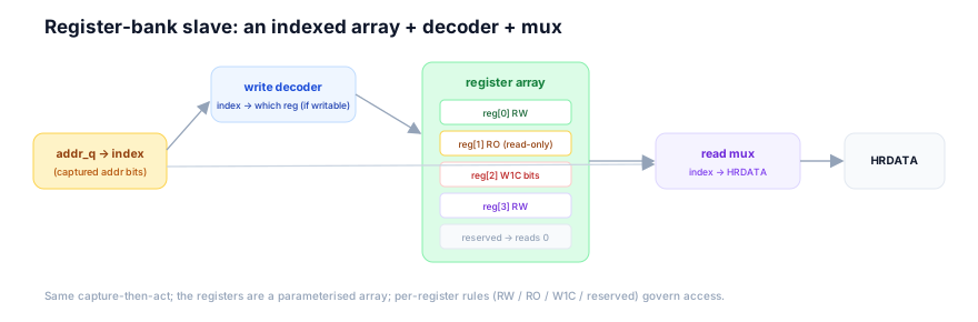
So a register bank slave is the simple slave (16.1) scaled and parameterised: the structure (capture-then-act, qualified select, registered context) is identical, but the storage becomes a configurable indexed array, and each register gains access attributes (it's not all plain RW). The write path becomes a decoder (index → which writable register), the read path a mux (index → which register's value). The attributes are where the peripheral semantics live — RO status, W1C flags, RC registers, reserved holes. The bank is parameterised (register count, data width) so it's reusable across peripherals. A register bank slave is therefore the simple slave generalised with per-register access rules — the workhorse peripheral interface.
2. Why Does It Exist?
The register bank slave exists because peripherals are controlled through registers — and they need many registers with varied semantics (control, status, flags, data), so a parameterised array with per-register attributes is the standard, reusable way to build that interface.
The register-based peripheral control is the root: a peripheral (UART, timer, GPIO, etc.) is controlled by software writing/reading its registers — a control register to configure it, a status register to read its state, data registers to send/receive, flag registers for interrupts. So every peripheral needs a register interface — a set of registers the CPU accesses over the bus. The register bank slave exists to provide that control surface.
The many registers, varied semantics drives the array + attributes: a peripheral has many registers (often dozens), and they have different semantics — control (RW — software sets), status (RO — hardware-driven, software reads), interrupt flags (W1C — hardware sets, software clears), FIFOs (RC or special), reserved (holes). So a single uniform "register" isn't enough — you need an array (for the many) with per-register attributes (for the varied semantics). The bank is therefore an indexed array with per-register attributes.
The parameterised reusability is why it's parameterised: every peripheral needs a register bank, with different counts, widths, and attributes. So building a parameterised register bank (configurable count/width/attributes) means the same RTL is reused across peripherals — you instantiate and configure it, rather than writing each from scratch. Parameterising it makes the same RTL reusable across peripherals, which is why register-bank generators are common. In summary, the register bank slave exists because: peripherals are controlled through registers (the why); they need many registers with varied semantics — control/status/flags/data (driving the indexed array with per-register attributes); and a parameterised bank is reusable across peripherals (the generalization). It is the standard, parameterised, reusable register-array interface that every peripheral uses. (The per-register attributes are where the peripheral's specific behavior lives, often generated from a register-map description — chapter 11.4 / IP-XACT/SystemRDL.)
3. Mental Model
Model the register bank as a wall of labeled mailboxes with different rules per box — most are normal boxes you can put mail in and take mail out (RW); some are "outgoing only" display boxes showing a notice you can read but not change (RO status); some are alarm boxes that light up when triggered and you reset by flipping their switch (W1C flags); some dispense a ticket that's consumed when you take it (RC); and some slots are just blanks in the wall (reserved — nothing there).
A wall of labeled mailboxes (the register array), each at a numbered slot (the index). You access them with a slot number (the captured address index). But the boxes have different rules. Most are normal mailboxes — you can put mail in (write) and take mail out (read), and what you put is what you get (RW registers). Some are "display only" boxes — they show a notice posted by the building (the hardware), which you can read but can't change — trying to "mail" something to them does nothing (RO status registers — ignore writes, read the hardware value). Some are alarm boxes that light up when an event triggers them (hardware sets the flag), and you reset the alarm by flipping its switch — specifically by writing a "1" to acknowledge it (W1C interrupt flags — hardware sets, software clears by writing 1). Some dispense a ticket that's consumed the moment you take it — reading it removes it (RC read-to-clear — clears on read, so you must be careful not to "peek" accidentally, which is why the qualified select matters — an idle glance shouldn't consume the ticket). And some slots are just blanks in the wall — nothing there (reserved — reads 0, ignores writes). So the wall is an array of slots with per-slot rules — and you access each by its number, respecting its rule.
This captures the register bank: the wall of numbered mailboxes = the indexed register array; the slot number = the captured address index (addr_q); normal put-in/take-out boxes = RW registers; display-only notice boxes = RO status (ignore writes); alarm boxes reset by flipping the switch = W1C flags (write 1 to clear); tickets consumed when taken = RC read-to-clear (clears on read); being careful not to peek-consume = qualifying the read so an idle cycle doesn't clear it; blank slots = reserved (reads 0). An array of slots with per-slot rules, accessed by number.
Watch a write to a RW register and a write-1-to-clear of a flag:
RW write, then W1C clear of a flag
4 cyclesThe model's lesson: an array of slots with per-slot rules, accessed by number. In the waveform, the RW register stores the write, and the W1C flag is cleared by writing a 1 — each register obeys its own attribute.
4. Real Hardware Perspective
In hardware, the register bank is a parameterised array of register flops, a write decoder (generating per-register write-enables, respecting writability), a read mux (selecting by index), and per-register attribute logic — often generated from a register-map description.
The parameterised array: the registers are declared as a parameterised array (e.g. reg [WIDTH-1:0] regs [0:COUNT-1], with WIDTH and COUNT as parameters). The same RTL therefore handles any count and width by parameter.
The write decoder and read mux: the write path is a decoder — in the data phase, if (sel_q && write_q), the index (addr_q) is decoded to a per-register write-enable: we[i] = (addr_q == i) && (register i is writable). Each register flop updates if (we[i]) regs[i] <= HWDATA (or, for W1C, the appropriate clear logic). The read path is a mux — HRDATA = regs[addr_q] (or the attribute-specific read value, e.g. 0 for reserved). In hardware the write path is a decoder generating write-enables and the read path a mux on the index.
The per-register attribute logic: each register's attribute shapes its logic. RW: plain — write-enable updates it, read returns it. RO: no write-enable (writes ignored); read returns the hardware-driven value (not a stored flop). W1C: hardware sets bits; a write with a 1 in a bit position clears that bit (if (we && HWDATA[b]) regs[i][b] <= 0); hardware-set otherwise. RC: cleared on read (the read access, qualified, triggers a clear — must qualify so an idle cycle doesn't clear it). Reserved: read returns 0, no write-enable. Each register's logic implements its own attribute. In hardware, then, the register bank is a parameterised flop array + a write decoder (per-register write-enables, respecting writability) + a read mux (by index) + per-register attribute logic (RW/RO/W1C/RC/reserved). Crucially, this is often generated — from a register-map description (IP-XACT, SystemRDL — chapter 11.4), a generator produces the bank RTL (with the right count/width/attributes) and the software headers, ensuring consistency. Register banks are therefore typically generated rather than hand-written, for consistency and productivity.
5. System Architecture Perspective
At the system level, the register bank is the standard control/status interface between software and hardware — and its per-register attributes and single-source generation (from a register map) are what make the hardware/software interface consistent and maintainable.
The software/hardware control interface: the register bank is the interface through which software controls and observes hardware. Software writes control registers to configure a peripheral, reads status registers to observe it, writes W1C flags to acknowledge interrupts, reads/writes data registers to transfer. So the register bank is the contract between the software (driver) and the hardware (peripheral). The register bank is the boundary where software meets hardware — the driver's view of the peripheral.
The attributes encode the contract: the per-register attributes (RW/RO/W1C/RC/reserved) encode the semantics of that contract — what each register means and how it behaves. RW = software-controllable setting; RO = hardware-reported status; W1C = interrupt acknowledge; RC = consume-on-read; reserved = don't-touch. So the attributes are the semantic specification of the interface — they tell the software how to use each register. So at the system level, the attributes are the documented behavior of the control interface. So they define the contract's semantics. So the attributes are the interface spec.
The single-source generation: because the register bank is the SW/HW contract, consistency between the hardware (the bank RTL) and the software (the driver's register definitions) is critical (chapter 11.4) — a mismatch (wrong attribute, wrong address) is a bug. So register banks are typically generated from a single register-map description (IP-XACT, SystemRDL): the generator produces the bank RTL (correct attributes/addresses), the software headers (matching addresses/fields), and the documentation — all from one source, guaranteeing consistency. So at the system level, the register bank (and its software interface) is generated from a single source for consistency and maintainability — a key SoC-design discipline. So at the system level, the register bank is the standard control/status interface between software and hardware (the SW/HW contract — the driver's view of the peripheral), its per-register attributes encode the semantic specification of that contract (RW/RO/W1C/RC/reserved — how to use each register), and it's typically generated from a single register-map source (consistency between RTL, headers, docs — chapter 11.4). So the register bank is where the bus's slave RTL meets the software interface — the most consequential slave type, because it's the control surface of every peripheral, and its correctness (attributes, addresses, generation) is foundational to a working, maintainable SoC. So it's the workhorse, generated, contract-defining interface. So get the register map right and generate from it.
6. Engineering Tradeoffs
The register bank embodies the indexed-array, per-register-attribute, parameterised-generated design.
- Parameterised array vs fixed registers. A parameterised array (configurable count/width) is reusable across peripherals at the cost of the parameterization; fixed registers (16.1) are simpler but not reusable. Parameterise for reuse.
- Per-register attributes vs uniform RW. Per-register attributes (RO/W1C/RC/reserved) match the peripheral's real semantics at the cost of attribute logic; treating all as RW is simpler but wrong (e.g. a status register isn't writable). Implement the attributes.
- Generated vs hand-written. Generating the bank (and headers) from a register-map description guarantees HW/SW consistency at the cost of the generation tooling; hand-writing risks mismatch bugs. Generate from a single source.
- Qualify reads (for RC) vs not. Qualifying reads (HSEL && real HTRANS) prevents read-to-clear registers being spuriously cleared by idle cycles (correct) at the cost of the qualification; not qualifying corrupts RC registers. Always qualify (especially for RC).
The throughline: a register bank slave generalizes the simple slave (16.1) into a parameterised indexed array of registers — the same capture-then-act structure (capture sel_q, write_q, the index from addr_q; act in the data phase), with a write decoder (index → which writable register receives HWDATA) and a read mux (index → the addressed register onto HRDATA). Each register has per-register access attributes — RW / RO / W1C / RC / reserved-reads-0 — encoding the peripheral's semantics. The bank is parameterised (count, width) and typically generated from a single register-map source (HW/SW consistency, chapter 11.4). Read-to-clear registers especially need the qualified select (so idle cycles don't spuriously clear them). It's the standard control/status interface — the SW/HW contract of every peripheral.
7. Industry Example
Build a register bank for a UART peripheral.
A UART has registers: CTRL (RW), STATUS (RO), TXDATA (W), RXDATA (RC — read pops the RX FIFO), IRQFLAGS (W1C), and reserved holes.
- The indexed array. The registers are an indexed array (by
addr_q, the captured address bits).CTRLat index 0,STATUSat 1,TXDATAat 2,RXDATAat 3,IRQFLAGSat 4, reserved elsewhere. - CTRL (RW). Writing CTRL configures the UART (baud, parity, enables) — a plain RW register: write-enable updates it, read returns it.
- STATUS (RO). STATUS reflects hardware state (TX empty, RX full, busy) — read-only: it has no write-enable (writes ignored), and reads return the hardware-driven value (not a stored flop). A write to STATUS does nothing (a robust bank might ERROR — chapter 16.6).
- RXDATA (RC, FIFO pop). Reading RXDATA returns the next received byte and pops the RX FIFO (a read side effect). Crucially, this pop is qualified: it triggers only on
sel_q = HSEL && real HTRANS(a real read). If it triggered onHSELalone, an IDLE cycle (withHSELhigh) would spuriously pop the FIFO — losing received data. The qualification prevents this. - IRQFLAGS (W1C). IRQFLAGS bits are set by hardware (on interrupt events). Software clears a flag by writing a 1 to it (write-1-to-clear):
if (we && HWDATA[b]) IRQFLAGS[b] <= 0(and hardware-set otherwise). So writing 0x04 to IRQFLAGS clears bit 2. - Reserved. Accessing a reserved index reads 0 and ignores writes (or ERRORs in a robust bank).
- Generated from a register map. The whole bank is generated from the UART's register-map description (SystemRDL/IP-XACT) — producing the bank RTL (with the right attributes), the software header (matching addresses/fields), and the docs — all consistent.
The example shows the register bank in action: an indexed array with per-register attributes (CTRL RW, STATUS RO, RXDATA RC with a qualified pop, IRQFLAGS W1C, reserved), built on the simple slave's capture-then-act, parameterised and generated from a single source. The qualified read protecting RXDATA's FIFO-pop is the critical detail. This is how a peripheral's register interface is built. This is the workhorse slave.
7b. The Bank, Written Out
Section 7 makes the right point about the RX FIFO pop — it must be qualified on
sel_q, a real transfer, so an IDLE cycle with HSEL high cannot consume data.
That is the first half of the rule and it is the half most designs get right.
The second half only appears once the bank inserts a wait state. sel_q stays
asserted for every cycle of a stretched data phase, so a side effect gated on
sel_q alone fires once per cycle rather than once per transfer. A three-cycle
read pops the FIFO three times and discards two bytes.
A side effect belongs to the transfer, not to the data phase. The cycle that
owns it is the one where the transfer actually completes: sel_q && HREADYOUT.
module ahb_regbank_rc #(
  parameter int AW = 32,
  parameter int DW = 32,
  // Cycles the RX FIFO needs before its data is valid. Non-zero is what makes
  // the side-effect timing observable at all - see the Debug Lab below.
  parameter int RD_WAITS = 2
) (
  input  logic          HCLK,
  input  logic          HRESETn,
  input  logic          HSEL,
  input  logic [1:0]    HTRANS,
  input  logic [AW-1:0] HADDR,
  input  logic          HWRITE,
  input  logic [2:0]    HSIZE,
  input  logic          HREADY,          // GLOBAL ready from the interconnect
  input  logic [DW-1:0] HWDATA,
  output logic          HREADYOUT,
  output logic [DW-1:0] HRDATA,
  output logic [1:0]    HRESP,
  // Hardware side
  input  logic [DW-1:0] hw_status,       // drives the RO register
  input  logic [DW-1:0] rx_fifo_data,    // head of the RX FIFO
  input  logic          rx_fifo_empty,
  output logic          rx_fifo_pop,     // ONE pulse per completed RXDATA read
  input  logic [DW-1:0] hw_irq_set,      // hardware sets IRQ flags
  output logic [DW-1:0] ctrl_o,
  output logic          cmd_pulse        // ONE pulse per completed CMD write
);
  localparam logic [1:0] RSP_OKAY = 2'b00, RSP_ERROR = 2'b01;
  localparam logic [2:0] SIZE_WORD = 3'b010;

  // Register map (word offsets)
  localparam logic [3:0] OFF_CTRL = 4'h0, OFF_STATUS = 4'h4, OFF_RXDATA = 4'h8,
                         OFF_IRQ  = 4'hC;
  // 0x10 is deliberately unmapped; 0x14 is the write-only command strobe.
  localparam logic [4:0] OFF_CMD  = 5'h14;

  // ── Address phase ───────────────────────────────────────────────────────
  wire ap_valid = HSEL && HTRANS[1];               // NONSEQ or SEQ
  // Accept a new address phase only when the bus advances AND we release.
  wire capture_en = HREADY && HREADYOUT;

  logic            dp_sel, dp_write;
  logic [AW-1:0]   dp_addr;
  logic [2:0]      dp_size;

  always_ff @(posedge HCLK or negedge HRESETn) begin
    if (!HRESETn) begin
      dp_sel <= 1'b0; dp_write <= 1'b0; dp_addr <= '0; dp_size <= '0;
    end else if (capture_en) begin
      dp_sel <= ap_valid; dp_write <= ap_valid && HWRITE;
      dp_addr <= HADDR;   dp_size  <= HSIZE;
    end
  end

  // ── Decode, and the two ways an access is illegal ───────────────────────
  wire sel_ctrl   = dp_sel && (dp_addr[4:0] == 5'(OFF_CTRL));
  wire sel_status = dp_sel && (dp_addr[4:0] == 5'(OFF_STATUS));
  wire sel_rxdata = dp_sel && (dp_addr[4:0] == 5'(OFF_RXDATA));
  wire sel_irq    = dp_sel && (dp_addr[4:0] == 5'(OFF_IRQ));
  wire sel_cmd    = dp_sel && (dp_addr[4:0] == OFF_CMD);
  wire mapped     = sel_ctrl | sel_status | sel_rxdata | sel_irq | sel_cmd;

  // This bank is word-only. A byte or halfword access to a 32-bit control
  // register is almost always a software bug rather than an intent, so it is
  // reported rather than silently widened - AMBA permits either, and reporting
  // is what turns a driver bug into a driver fix.
  wire misaligned = dp_sel && ((dp_size != SIZE_WORD) || (dp_addr[1:0] != 2'b00));
  wire err_req    = dp_sel && (!mapped || misaligned);

  // ── Wait-state generation: only the RX FIFO path is slow ────────────────
  logic [$clog2(RD_WAITS+1)-1:0] wait_cnt;
  wire  needs_wait = sel_rxdata && !dp_write && !err_req && (RD_WAITS != 0);

  always_ff @(posedge HCLK or negedge HRESETn)
    if (!HRESETn)          wait_cnt <= '0;
    else if (!dp_sel)      wait_cnt <= '0;
    else if (needs_wait && wait_cnt != RD_WAITS[$bits(wait_cnt)-1:0])
                           wait_cnt <= wait_cnt + 1'b1;
    else if (HREADYOUT)    wait_cnt <= '0;

  // Two-cycle ERROR sequence for an illegal access.
  typedef enum logic [1:0] { E_OK, E_ERR1, E_ERR2 } estate_e;
  estate_e estate;

  always_ff @(posedge HCLK or negedge HRESETn)
    if (!HRESETn) estate <= E_OK;
    else unique case (estate)
      E_OK  : estate <= err_req ? E_ERR1 : E_OK;
      E_ERR1: estate <= E_ERR2;
      E_ERR2: estate <= E_OK;
    endcase

  assign HREADYOUT = (estate == E_ERR1) ? 1'b0
                   : (estate == E_ERR2) ? 1'b1
                   : !(needs_wait && wait_cnt != RD_WAITS[$bits(wait_cnt)-1:0]);

  assign HRESP = (estate == E_ERR1 || estate == E_ERR2) ? RSP_ERROR : RSP_OKAY;

  // ── THE completion cycle. Every side effect hangs off this and only this.
  wire complete = dp_sel && HREADYOUT && (estate == E_OK);
  wire do_write = complete &&  dp_write;
  wire do_read  = complete && !dp_write;

  // ── Registers ───────────────────────────────────────────────────────────
  logic [DW-1:0] ctrl_q, irq_q;

  always_ff @(posedge HCLK or negedge HRESETn) begin
    if (!HRESETn) begin
      ctrl_q <= '0; irq_q <= '0; rx_fifo_pop <= 1'b0; cmd_pulse <= 1'b0;
    end else begin
      // RW
      if (do_write && sel_ctrl) ctrl_q <= HWDATA;

      // W1C: hardware sets, a written 1 clears. Set wins on a tie, otherwise
      // an event arriving in the same cycle as its acknowledgement is lost.
      irq_q <= (irq_q & ~((do_write && sel_irq) ? HWDATA : '0)) | hw_irq_set;

      // RC: the FIFO pop is a SIDE EFFECT of a completed read. Gating it on
      // do_read - which carries HREADYOUT - makes it fire exactly once per
      // transfer regardless of how many wait states the data phase took.
      rx_fifo_pop <= do_read && sel_rxdata && !rx_fifo_empty;

      // WO command strobe: one pulse per completed write.
      cmd_pulse   <= do_write && sel_cmd;
    end
  end

  assign ctrl_o = ctrl_q;

  // ── Read mux. RO reads the hardware value, not a stored flop. WO and
  //    reserved read as zero rather than X, so a failure is reproducible.
  always_comb begin
    HRDATA = '0;
    if (dp_sel && !dp_write) begin
      unique case (1'b1)
        sel_ctrl  : HRDATA = ctrl_q;
        sel_status: HRDATA = hw_status;
        sel_rxdata: HRDATA = rx_fifo_data;
        sel_irq   : HRDATA = irq_q;
        default   : HRDATA = '0;          // WO, reserved, unmapped
      endcase
    end
  end
endmodule
Assertions that pin the side effects down
module ahb_regbank_rc_sva (
  input logic HCLK, HRESETn, HREADYOUT, rx_fifo_pop, cmd_pulse,
  input logic dp_sel, dp_write, sel_rxdata, sel_cmd, rx_fifo_empty
);
  // A pop may only occur in response to a COMPLETING read of RXDATA. This is
  // the property the wait-state bug violates: with the bug, pops occur on
  // cycles where HREADYOUT is low.
  a_pop_only_on_complete: assert property (@(posedge HCLK) disable iff (!HRESETn)
    rx_fifo_pop |-> $past(dp_sel && !dp_write && sel_rxdata && HREADYOUT))
    else $error("RX FIFO popped outside a completing read");

  // ...and at most once per transfer. Two pops without an intervening
  // completion means the data phase was counted more than once.
  a_pop_once: assert property (@(posedge HCLK) disable iff (!HRESETn)
    rx_fifo_pop |=> !rx_fifo_pop until_with (dp_sel && HREADYOUT));

  a_cmd_once: assert property (@(posedge HCLK) disable iff (!HRESETn)
    cmd_pulse |=> !cmd_pulse);

  // Never pop an empty FIFO.
  a_no_pop_empty: assert property (@(posedge HCLK) disable iff (!HRESETn)
    rx_fifo_pop |-> !$past(rx_fifo_empty));

  // Coverage: a pass means nothing if no waited read was ever issued.
  c_waited_read: cover property (@(posedge HCLK) disable iff (!HRESETn)
    dp_sel && !dp_write && sel_rxdata && !HREADYOUT);
endmodule
c_waited_read is the one to check first in a report. If it never hits, the
regression only ever issued zero-wait reads, and the side-effect timing this
whole section is about was never exercised.
Two out of every three received bytes vanished, and only on a busy bus
SIDE-EFFECT-PER-WAIT-CYCLEA UART driver lost received characters. The loss was not random: reading the RX data register returned the correct byte, and the next two bytes in the stream were gone — a repeating keep-one-drop-two pattern. Retransmission recovered the data, so the link worked and the throughput was a third of expected.
It reproduced only under load. A single read issued from a halted debugger returned every byte correctly, and the peripheral's own block-level regression was clean over millions of cycles.
// The pop was qualified on a real transfer - correctly - but not on the
// cycle that transfer completes.
always_ff @(posedge HCLK or negedge HRESETn)
  if (!HRESETn) rx_fifo_pop <= 1'b0;
  else          rx_fifo_pop <= dp_sel && !dp_write && sel_rxdata;
//                             ^^^^^^ true for EVERY cycle of a stretched
// data phase, not just the completing oneA waveform of one read made the count explicit:
  cycle           1      2      3      4
  dp_sel          0      1      1      1
  HREADYOUT       1      0      0      1     <- RD_WAITS = 2
  rx_fifo_pop     0      1      1      1     <- three pops, one transfer
  rx_level        5      4      3      2     <- FIFO drained by three
  HRDATA          -      -      -      B0    <- master samples one byte
Three pops for one read. The master sampled HRDATA on the single cycle where
HREADYOUT was high and saw one byte; the other two were removed from the FIFO
and never presented to anyone.
The keep-one-drop-two ratio in the symptom is RD_WAITS + 1 — a direct readout
of the wait-state count, which is what identified the mechanism before anyone
opened the RTL. The load dependence follows too: a debugger-driven single read
still popped three times, but with an idle link there were no queued bytes to
lose.
dp_sel identifies the transfer; it does not identify the cycle on which that
transfer completes. During a stretched data phase it stays asserted for every
wait cycle, so a side effect gated on it alone repeats once per cycle.
Section 7 gets the first half of this right — qualifying on a real HTRANS
prevents an IDLE cycle from popping the FIFO — and that qualification is
necessary but not sufficient. The complete rule needs both terms: the access
must be a real transfer and it must be the cycle that transfer completes,
which is dp_sel && HREADYOUT.
The reason a zero-wait bank never exposes this is that dp_sel and
dp_sel && HREADYOUT are the same signal when HREADYOUT is permanently high.
Every read-to-clear, FIFO-pop-on-read, clear-on-read status bit and write-triggered
command strobe in a zero-wait design is therefore correct by accident, and stays
correct right up until someone adds a wait state — for a slower FIFO, a clock
crossing, an ECC check — at which point every side-effecting register in the bank
breaks at once, and none of them changed.
// The completion cycle - the one cycle the transfer commits.
wire complete = dp_sel && HREADYOUT && (estate == E_OK);
wire do_read  = complete && !dp_write;

always_ff @(posedge HCLK or negedge HRESETn)
  if (!HRESETn) rx_fifo_pop <= 1'b0;
  else          rx_fifo_pop <= do_read && sel_rxdata && !rx_fifo_empty;
The test that fails on the old RTL and passes on the new one is a waited read
that counts pops: fill the FIFO, issue one RXDATA read with RD_WAITS = 2, and
assert that rx_fifo_pop asserted exactly once and the FIFO level dropped by
exactly one. The original verification plan had no such test because the bank was
zero-wait when it was written.
The durable guard is the assertion pair from the previous section — a pop must
follow a completing read, and no second pop may occur before the next completion
— together with c_waited_read to prove the regression actually issued a waited
read. An exactly-once assertion over a run containing only zero-wait reads is
vacuously satisfied.
The rule generalises to every side-effecting access: read-to-clear status bits, FIFO pops, write-triggered command strobes, and interrupt acknowledgements are all transfer events, not data phase events. Gate them on completion. For the wait-state contract itself see slave-inserted wait states, and for the capture discipline the completion term builds on, address / control capture.
8. Common Mistakes
9. Interview Insight
Register bank design is a practical RTL interview topic — the indexed-array structure, the per-register attributes, and the qualify-reads-for-RC point are the signals.
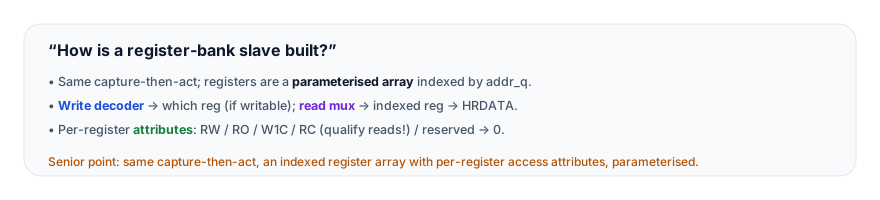
The answer that lands gives the structure and the attributes: "A register bank slave is the simple slave generalized into a parameterised array of registers, indexed by the captured address bits. It keeps the same capture-then-act structure — capture the qualified select, the write flag, and the register index in the address phase, then act in the data phase — but now the write path is a decoder, generating a per-register write-enable from the index, and the read path is a mux selecting the indexed register onto HRDATA. The key thing is that registers have per-register access attributes, not all plain read-write. A read-write register stores writes and returns them. A read-only register, like a status register, ignores writes and returns the hardware-driven value. A write-one-to-clear register, like interrupt flags, is set by hardware and cleared when software writes a 1 to the bit. A read-to-clear register clears itself when read. And reserved indices read as 0 and ignore writes. The bank is parameterised by register count and width for reuse, and it's usually generated from a register-map description like SystemRDL or IP-XACT, which produces the RTL, the software headers, and the docs from one source, keeping hardware and software consistent. One critical detail: registers with read side effects — read-to-clear, or reads that pop a FIFO — must use the qualified select, HSEL AND a real HTRANS, because if you triggered the side effect on HSEL alone, an idle cycle with HSEL high would spuriously clear or pop them, corrupting state. That's a classic bug — mysterious lost interrupts or data under load." The indexed-array structure, the per-register attributes, and the qualify-reads-for-RC point are the senior signals.
10. Practice Challenge
Build and reason from the register bank.
- The structure. Describe the register bank: indexed array, write decoder, read mux, on the simple slave's capture-then-act.
- Attributes. Describe the per-register attributes (RW/RO/W1C/RC/reserved) and a register example of each.
- Read the waveform. From Figure 2, explain the RW write and the W1C clear.
- Qualify for RC. Explain why read-to-clear registers must use the qualified select and the bug otherwise.
- Generation. Explain why register banks are generated from a register-map description.
11. Key Takeaways
- A register bank slave generalizes the simple slave into a parameterised indexed array of registers — same capture-then-act, but a write decoder (index → which writable register gets
HWDATA) and a read mux (index → the addressed register ontoHRDATA). - Per-register access attributes encode the peripheral's semantics: RW (plain), RO (status — ignore writes, read HW value), W1C (flags — HW sets, write 1 clears), RC (read-to-clear), reserved (reads 0).
- Read-to-clear / side-effecting registers MUST use the qualified select — an unqualified read spuriously clears/pops them on IDLE cycles (corrupting state — lost flags/data). Critical bug to avoid.
- It's parameterised (count, width) for reuse across peripherals — and typically generated from a single register-map source (SystemRDL/IP-XACT → consistent RTL + headers + docs, chapter 11.4).
- It's the SW/HW control contract — the standard control/status interface, the driver's view of every peripheral; the attributes are the interface's semantic spec.
- Reserved registers read 0 and ignore writes (a defined, safe behavior) — not random (or ERROR in a robust bank).
11b. Where This Is Specified
- Arm AMBA 5 AHB Protocol Specification (ARM IHI 0033). The address-phase/data-phase pipeline,
HREADYversus a subordinate'sHREADYOUT, the requirement that a manager holds its address phase while stalled, the transfer-size encoding onHSIZEand the alignment rule, and the two-cycle ERROR response used here for unmapped and misaligned accesses. - Arm AMBA 3 AHB-Lite Protocol Specification (ARM IHI 0033A). Slave-inserted wait states and the
HREADYOUTcontract for the single-manager subset. - IEEE 1800-2023 §16 — Assertions. The concurrent properties and
cover propertyused for the exactly-once side-effect checks, includinguntil_with. - IEEE 1800-2023 §27 — Generate constructs. The elaboration used by parameterised register arrays.
Register-map description languages (SystemRDL, IP-XACT) and the generators that emit bank RTL plus matching software headers are industry practice rather than standardised behaviour, and are documented per tool.
12. What Comes Next
You now can build a parameterised register bank. The next chapter adds wait states for larger/slower storage:
- Memory Slave (next) — an AHB SRAM/memory slave with wait states.
- HREADYOUT Generation, HRDATA Muxing, HRESP Generation, and the rest — the richer slave RTL.
To revisit the simple slave this extends, see A Simple AHB-Lite Slave; for the register map driving generation, see The Address Map.