An I²C controller is a serial two-wire master engine wrapped in an APB register file — and its defining subtlety is that the same APB offset means a different register depending on whether you read or write it. Firmware never bit-bangs SCL and SDA directly; it programs a small bank of control/status registers (CSRs) over APB, and a hardware byte-engine turns those register writes into the open-drain start/address/data/stop waveform on the wire. The map is the widely-deployed OpenCores I²C master (Richard Herveille): a clock prescale pair (PRERlo/PRERhi), a control register (CTR), a transmit/receive byte register that is TXR on write and RXR on read at the same offset, and a command/status register that is CR on write and SR on read at the same offset. The single idea to carry: on this peripheral the APB decode must branch on PWRITE, not just PADDR — if (pwrite) reg_txr <= pwdata; else prdata <= rxr; — because read and write at one offset hit two physically different registers. Get that wrong and you read back your own command bits as status, or you read stale transmit data as received data.
1. Problem statement
The problem is driving a slow, open-drain, two-wire serial bus (I²C) from a synchronous parallel CPU bus (APB) without making firmware toggle every clock edge — and doing it through a register interface compact enough that the same offset has to serve two registers.
I²C is a deliberately minimal protocol — two wires, SCL (clock) and SDA (data), both open-drain and pulled high — running at 100 kHz, 400 kHz, or 1 MHz, far slower than PCLK. A transaction is a precise sequence of bit-level events: a START condition (SDA falling while SCL is high), eight clocked address bits plus a read/write bit, an acknowledge bit driven by the slave, then data bytes each followed by an ACK, and finally a STOP condition (SDA rising while SCL is high). Three things make this hard to expose over APB:
- The timing is bit-level and slow; the CPU bus is word-level and fast. Firmware cannot afford to drive each of the millions of
SCL/SDAedges per second by hand — it would consume the CPU. The controller must generate the bit timing in hardware from a divider and run a byte-level command engine, so firmware issues "send this byte, then ACK" and the hardware produces the dozens of edges. - The bus is open-drain and multi-master; the controller must observe, not just drive.
SDAis driven low or released-high, never driven high — so the slave's ACK, and another master's contention (arbitration), are things the controller must read back from the wire. Status (RxACK,AL,BUSY,TIP) is therefore as important as command. - The register budget is tiny, so offsets are overloaded. A minimal I²C master exposes only a handful of registers. To keep the map small, the transmit and receive bytes share one offset (write = transmit, read = receive), and the command and status registers share another (write = command, read = status). That overloading is efficient but it makes the APB decode direction-dependent, which is the recurring trap.
So the job is not "store a byte" — it is to build an APB slave that decodes by direction, generates I²C bit timing from a prescale divider, runs a command-driven byte engine (START → address+RW → data → STOP), and exposes the wire's response as pollable status — all behind six register offsets.
2. Why previous knowledge is insufficient
The earlier chapters built every primitive this controller uses — but each assumed an offset is one register with one meaning, and an I²C master breaks exactly that assumption while adding a serial engine no CSR chapter covered.
- CSR fundamentals and the register-bank design assumed one offset, one register. They taught RW/RO/WO access types and how to lay out a bank — but always with
PADDRselecting a single flop whose access type is fixed. Here the same offset is a write-onlyTXRand a read-onlyRXR, or a write-onlyCRand a read-onlySR. The access type is not a property of the offset; it is a property of the offset and the direction. That is a decode the prior banks never had to make. - Write logic and the read-data mux were built independently. Write logic committed
pwdatato a flop selected byPADDR; the read mux selected a flop ontoPRDATAbyPADDR. On this peripheral those two decoders select different registers at the same address — the write path of offset0x3lands inTXR, the read path of offset0x3sources fromRXR. The two decoders must be designed together and gated onPWRITE, not bolted on independently. - The write-only and read-only register chapters taught each in isolation. A write-only register reads back as zero or garbage; a read-only register ignores writes. I²C pairs a write-only and a read-only register at one offset — so the "reads as zero" behaviour of
TXRis replaced by "reads asRXR," and the "ignores writes" behaviour ofSRis replaced by "writes go toCR." The peripheral composes the two patterns onto one address. - No prior chapter generated a serial protocol. The prescale divider (
PCLK/(5×SCL)−1), the bit-levelSCL/SDAshifter, and the START/WRITE/READ/STOP command engine are new machinery. They sit behind the CSR file — firmware touches only the registers — but they are what make this a peripheral and not just a register bank.
So the model to add is the direction-decoded register file driving a serial command engine: an APB slave whose decode branches on PWRITE, feeding a prescale-clocked byte engine that produces the I²C waveform and reports the wire back as status. This is the same family as the UART APB interface — a CSR-fronted serial peripheral — applied to I²C's two-wire, open-drain, command-and-poll discipline.
3. Mental model
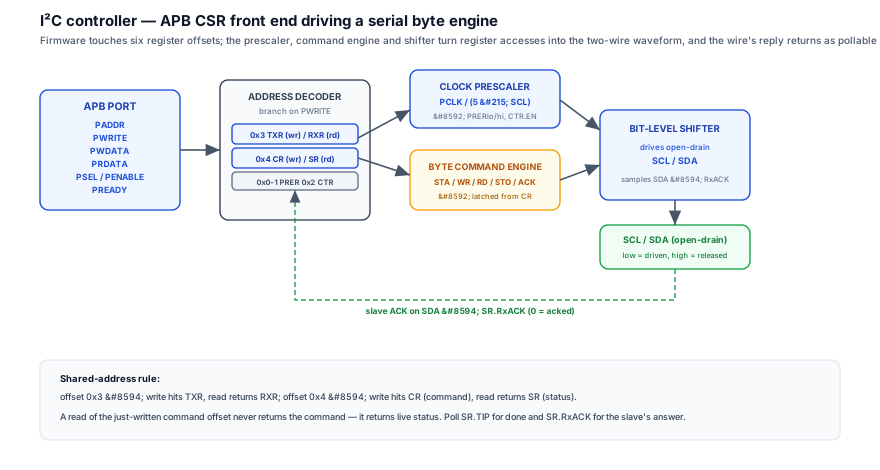
The model: the I²C controller is a vending machine with six buttons, where two of the buttons do one thing when you push them (write) and show something else when you look at them (read). Firmware loads a coin (the prescale, the enable), presses a button labelled with a byte (write TXR), presses a command button (write CR with START+WRITE), then watches the same command button's face for the result (read SR: transfer-in-progress, then ack-received). The wire-level mechanics — the start condition, the eight clocked bits, the ack — all happen inside the machine; firmware only loads, commands, and polls.
Four refinements make it precise:
- The prescale sets the gear ratio between
PCLKandSCL.PRER(PRERlo+PRERhi, 16 bits) holdsprescale = PCLK/(5×SCL) − 1. The internal bit-engine clock runs at5×SCL(the master needs ~5 internal ticks perSCLperiod to place edges, sample, and meet setup/hold), so dividingPCLKdown by5×SCLand subtracting one (because the counter counts from zero) gives the reload value. Program it once at init like any clock-divider configuration; it is set-once state. - The command register is a trigger, not a value. Writing
CRdoes not store a number you read back — it launches an action.STArequests a START,WRrequests "transmit the byte inTXR,"RDrequests "receive a byte,"STOrequests a STOP,ACKchooses the ack the master sends after a read, andIACKacknowledges the interrupt. The bits are self-clearing as the engine consumes them. That is why reading theCRoffset returnsSRinstead — there is no stored command word to read. - Status is the wire, read back.
SRreflects the physical bus:TIP(transfer in progress — the engine is mid-byte),RxACK(the ack bit the slave returned: 0 = ACK, 1 = NACK / no slave),BUSY(a START seen, no STOP yet),AL(arbitration lost to another master), andIF(interrupt flag). Firmware pollsTIPto wait for a byte to finish, then checksRxACKto know whether a slave answered. - The whole APB-facing job reduces to: load
PRER, enable inCTR, then loop (writeTXR, writeCR, pollSR.TIP, checkSR.RxACK). Everything else is the engine's problem. The model firmware carries is the register protocol, not the wire protocol.
4. Real SoC implementation
Here is the OpenCores I²C master register map exposed over APB, followed by the APB decode that makes the shared offsets work. The map is the load-bearing artifact — note the two rows that share an offset and differ only by access direction.
| Offset | Name (write / read) | Access | Reset | Purpose |
|---|---|---|---|---|
0x00 | PRERlo | RW | 0xFF | Clock prescale, low byte — prescale[7:0] of PCLK/(5×SCL)−1 |
0x01 | PRERhi | RW | 0xFF | Clock prescale, high byte — prescale[15:8] |
0x02 | CTR | RW | 0x00 | Control: EN (bit 7, core enable), IEN (bit 6, interrupt enable) |
0x03 | TXR (write) | WO | 0x00 | Transmit byte: 7-bit slave address + R/W bit (first byte), or data |
0x03 | RXR (read) | RO | 0x00 | Received byte from the last read — same offset as TXR, read direction |
0x04 | CR (write) | WO | 0x00 | Command: STA start, STO stop, RD read, WR write, ACK, IACK |
0x04 | SR (read) | RO | 0x00 | Status: RxACK, BUSY, AL, TIP, IF — same offset as CR, read direction |
// I2C master CSR file over APB. The non-trivial point: offsets 0x3 and 0x4
// are DIFFERENT registers on read vs write, so the decode branches on PWRITE.
//
//   0x0 PRERlo  RW   prescale[7:0]
//   0x1 PRERhi  RW   prescale[15:8]    prescale = PCLK/(5*SCL) - 1
//   0x2 CTR     RW   {EN, IEN, ...}    core enable / interrupt enable
//   0x3 TXR(w)/RXR(r) WO/RO            write = byte to transmit, read = byte received
//   0x4 CR(w) /SR(r)  WO/RO            write = command, read = status

localparam ADDR_PRERLO = 3'h0, ADDR_PRERHI = 3'h1, ADDR_CTR = 3'h2,
           ADDR_TXR_RXR = 3'h3, ADDR_CR_SR = 3'h4;

logic [15:0] prer;          // PRERhi:PRERlo concatenated prescale value
logic [7:0]  ctr;           // control: ctr[7]=EN, ctr[6]=IEN
logic [7:0]  txr;           // transmit byte (write-only at 0x3)
logic [7:0]  rxr;           // received byte (read-only at 0x3) — driven by the engine
logic [7:0]  cr;            // latched command pulse (write-only at 0x4)

// status bits assembled from the byte engine (read-only at 0x4)
wire  [7:0]  sr = {rxack, 1'b0, al, busy, 4'b0, tip, irq_flag}[7:0]; // see note below
wire         wr_en = psel && penable && pwrite && pready;  // APB write commit
wire         rd_en = psel && penable && !pwrite;           // APB read

// ---- WRITE PATH: PADDR selects, but TXR/CR only exist on the write side ----
always_ff @(posedge pclk or negedge presetn) begin
  if (!presetn) begin
    prer <= 16'hFFFF;       // reset prescale: slowest SCL, safe default
    ctr  <= 8'h00;          // core disabled out of reset
    txr  <= 8'h00;
    cr   <= 8'h00;
  end else begin
    cr <= 8'h00;            // CR is a self-clearing command pulse: 1 cycle wide
    if (wr_en) unique case (paddr[2:0])
      ADDR_PRERLO : prer[7:0]  <= pwdata[7:0];   // lower prescale byte
      ADDR_PRERHI : prer[15:8] <= pwdata[7:0];   // upper prescale byte
      ADDR_CTR    : ctr        <= pwdata[7:0];   // EN / IEN
      ADDR_TXR_RXR: txr        <= pwdata[7:0];   // WRITE 0x3 -> TXR (transmit byte)
      ADDR_CR_SR  : cr         <= pwdata[7:0];   // WRITE 0x4 -> CR  (command latch)
      default     : ;                            // reserved: ignore
    endcase
  end
end

// ---- READ PATH: SAME offsets 0x3 / 0x4 source RXR / SR, never TXR / CR ----
always_comb begin
  prdata = 32'h0;
  if (rd_en) unique case (paddr[2:0])
    ADDR_PRERLO : prdata = {24'h0, prer[7:0]};
    ADDR_PRERHI : prdata = {24'h0, prer[15:8]};
    ADDR_CTR    : prdata = {24'h0, ctr};
    ADDR_TXR_RXR: prdata = {24'h0, rxr};   // READ 0x3 -> RXR (received byte), NOT txr
    ADDR_CR_SR  : prdata = {24'h0, sr};    // READ 0x4 -> SR  (status),        NOT cr
    default     : prdata = 32'h0;
  endcase
end
// The shared-address rule in one line, the way real RTL writes it:
//   if (pwrite) reg_txr <= pwdata;  else  prdata <= rxr;   // for offset 0x3
//   if (pwrite) cr      <= pwdata;  else  prdata <= sr;    // for offset 0x4

// ---- PRESCALE DIVIDER: counts PCLK down to the 5*SCL internal bit clock ----
// prer holds PCLK/(5*SCL) - 1, so a free-running counter reloads at 0 and the
// terminal-count strobe is the internal bit-engine tick.
logic [15:0] pre_cnt;
wire         bit_tick = (pre_cnt == 16'h0);
always_ff @(posedge pclk or negedge presetn)
  if (!presetn)        pre_cnt <= 16'h0;
  else if (!ctr[7])    pre_cnt <= 16'h0;          // EN=0: divider held in reset
  else if (bit_tick)   pre_cnt <= prer;           // reload from prescale value
  else                 pre_cnt <= pre_cnt - 16'h1;

// ---- COMMAND LATCH: the byte engine consumes cr's STA/WR/RD/STO/ACK pulse ----
// cr is one cycle wide (cleared above); the engine captures the request and runs
// the START -> address+RW -> data -> STOP sequence on SCL/SDA at bit_tick rate,
// driving rxr (received byte), rxack (slave ack), tip, busy, al back to the CSRs.
Three facts make this the correct shape. First, the decode is direction-dformed: the write always_ff and the read always_comb are two separate decoders, and at offsets 0x3/0x4 they deliberately select different registers — TXR/CR on write, RXR/SR on read. Writing this as one PADDR-only mux (the natural instinct from the single-register banks) is the canonical bug on this peripheral: you would read back your last command in CR as if it were status, or read your transmit byte as if it were the received byte. Second, CR is a self-clearing pulse, not stored state — it is forced to 0 every cycle and only momentarily carries the STA/WR/STO request, which is why the read side of 0x4 cannot return CR (there is nothing to return) and returns SR instead. Third, the prescale divider is the bridge between the two clock worlds: prer = PCLK/(5×SCL)−1 feeds a counter whose terminal count is the internal bit clock, gated by CTR.EN so a disabled core holds the divider in reset and the wire idle. The commit machinery underneath is still the write logic and read-data mux — this peripheral only makes their selection depend on PWRITE.
5. Engineering tradeoffs
The register map is the engineering artifact, and its central decision is the address overloading. The table makes the tradeoff explicit, register by register.
| Register (offset) | Access design | Why this choice | Tradeoff / risk |
|---|---|---|---|
PRERlo/PRERhi (0x0/0x1) | RW, 16-bit prescale split over two byte offsets | Keeps the bus 8-bit-friendly; set once at init like a clock-divider config | A non-atomic two-write update can momentarily mis-clock if EN is high; program prescale before enabling |
CTR (0x2) | RW, EN/IEN | One control word; readable so firmware confirms the core is enabled | Enabling with a bad prescale runs SCL at the wrong rate — order matters |
TXR/RXR (0x3) | WO write / RO read at one offset | Saves an address; transmit and receive are never needed simultaneously on a half-duplex wire | Read-of-write-offset trap: reading 0x3 returns RXR, not the byte you wrote — easy to assume readback |
CR/SR (0x4) | WO write / RO read at one offset | A command is a one-shot pulse with no value to store, so the read side is free for status | Reading 0x4 returns SR; firmware that expects to read its command back gets status bits instead |
SR fields (0x4 read) | RO status assembled from the wire | RxACK/TIP/BUSY/AL are physical bus state, hardware-owned, status-register style | Polling-only; a poll loop that ignores AL misses arbitration loss on a multi-master bus |
The throughline: the address overloading buys a smaller map at the cost of a direction-dependent decode and a firmware trap. The win is real — six offsets instead of eight, an 8-bit-clean layout — and it is the historically standard I²C-master map, so firmware and verification IP already expect it. The cost is concentrated in one place: a developer who treats the map like an ordinary register bank — where an offset is one register — will read 0x3 expecting their transmit byte and get the received byte, or read 0x4 expecting their command and get status. The mitigation is documentation and a decode that is explicitly gated on PWRITE, plus an assertion that a read of 0x4 returns SR and never the last CR value. Compared with giving each register its own offset (simpler decode, no trap, but a larger map and a break from the de-facto-standard layout), the shared-offset map is the right call because it is the standard — but only if the decode and the docs make the direction-dependence unmissable.
6. Common RTL mistakes
7. Debugging scenario
The signature I²C-controller bug is a decode that ignores PWRITE, so a read of the command offset returns the last command instead of status — firmware polls 0x4 for TIP, reads back its own CR bits, misreads them as status, and either spins forever or charges ahead into a corrupt transfer.
-
Observed symptom: firmware writes the slave address to
TXR, writesCR = STA|WRto start the transfer, then polls offset0x4waiting forTIPto clear. The poll never sees the expected status pattern — sometimes it reads a value that looks like the transfer is permanently in progress, sometimes it reads theSTA|WRbits it just wrote and misinterprets them, and the driver either hangs in the poll loop or proceeds to write the next byte while the previous one is still on the wire, garbling it. It works in a unit test that only ever writes registers and never reads them back. -
Waveform clue: on the APB trace, a write to
PADDR = 0x4(PWRITE = 1) carryingPWDATA = 0x90(STA|WR) commits into thecrflop — correct. One cycle later a read toPADDR = 0x4(PWRITE = 0) drivesPRDATAwith0x90— the command value, not the assembledSRstatus word. The read decoder selectedcron offset0x4regardless of direction; it never branched onPWRITE, so the read side returned the write-side register. -
Root cause: the address decoder was written as a single
PADDR-only mux — the natural pattern from an ordinary register bank where one offset is one register — so offset0x4selected thecrflop for both read and write. The shared-address-by-direction rule of the I²C map was not honoured: the read of0x4must sourceSR, but the decoder sourcedCR. (The same defect on0x3would returnTXRon a read instead ofRXR.) -
Correct RTL: split the decode and gate the shared offsets on
PWRITE, so the read side of0x3/0x4sourcesRXR/SRand never the write-side register:Azvya Education Pvt. Ltd.VLSI MentorSnippet// SHARED-OFFSET DECODE — branch on PWRITE for offsets 0x3 and 0x4. always_comb begin prdata = 32'h0; if (psel && penable && !pwrite) unique case (paddr[2:0]) 3'h3 : prdata = {24'h0, rxr}; // read 0x3 -> RXR (received), never TXR 3'h4 : prdata = {24'h0, sr}; // read 0x4 -> SR (status), never CR // ... other read-only sources ... default : prdata = 32'h0; endcase end // write side (separate decoder) lands 0x3 -> TXR, 0x4 -> CR, on PWRITE only. -
Verification assertion: prove the read of the
CR/SRoffset returns status and never the last command written, and that launching a transfer setsTIP:Azvya Education Pvt. Ltd.VLSI MentorSnippet// A read of offset 0x4 must return SR, NOT the value last written to CR. property p_read_cr_offset_is_status; @(posedge pclk) disable iff (!presetn) (psel && penable && !pwrite && paddr[2:0]==3'h4) |-> (prdata[7:0] == sr); endproperty a_read_cr_is_status: assert property (p_read_cr_offset_is_status); // Writing CR with STA|WR while enabled launches a transfer: TIP must rise. property p_cmd_launches_transfer; @(posedge pclk) disable iff (!presetn) (wr_en && paddr[2:0]==3'h4 && pwdata[7] && pwdata[4] && ctr[7]) |-> ##[1:8] tip; endproperty a_cmd_sets_tip: assert property (p_cmd_launches_transfer); -
Debug habit: when an I²C poll loop hangs or a transfer corrupts, do not start in the byte engine — first check the decode direction at the shared offsets. Capture a read of
0x4right after aCRwrite and confirmPRDATAcarries theSRstatus word, not theCRbits. A huge fraction of "I²C never completes" bugs are aPADDR-only decoder that returns the command offset's write register on a read — the fix is to gate the shared offsets onPWRITE, not to debug the wire.
8. Verification perspective
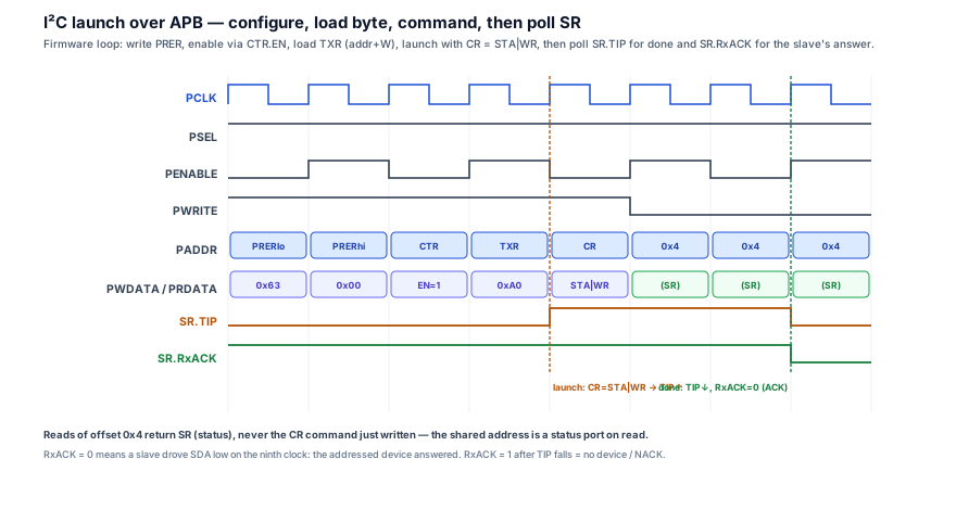
The I²C controller's verification splits into two halves: proving the APB CSR contract (especially the shared-address direction decode) and proving the byte engine turns commands into the right wire sequence and status. The high-value APB-side checks live on the shared offsets and the command-to-status causality.
- The shared-offset direction decode is the headline property. Assert that a read of offset
0x4returnsSRand never the last value written toCR—(read && paddr==0x4) |-> prdata[7:0]==sr— and the analogous property that a read of0x3returnsRXR, notTXR. Pair it with a negative check: a write to0x4must not appear on a subsequent read of0x4(the command does not read back). These two catch thePADDR-only-decoder bug that is the peripheral's defining defect; an ordinary register-bank test suite that assumes write-then-read-returns-the-write would pass on broken RTL, so the direction check must be explicit. - Command-launches-transfer is the causal liveness property. Writing
CRwithSTA|WRwhileCTR.ENis set must setTIPwithin a few cycles —(wr_cr && STA && WR && EN) |-> ##[1:N] tip— andTIPmust eventually fall (bounded-liveness, like the wait-state watchdog discipline) so a hung engine becomes a loud failure rather than a silent spin. Cover bothRxACK=0(slave present) andRxACK=1(no slave / NACK) so the missing-slave path is exercised, not just the happy path. - The self-clearing command pulse needs its own check. Assert
CRis one cycle wide — writtenSTA|WRthis cycle, zero the next — so the engine sees a clean one-shot and a second transfer is not accidentally re-triggered by a sticky command. This is the property that fails if someone makesCRa stored RW register by mistake. - The prescale must be programmed-before-enabled, and
SCLmust match it. A directed test that setsPRERthenENand measures the resultingSCLperiod confirmsprescale = PCLK/(5×SCL)−1; a test that enables with a stalePRERconfirms the documented (mis-clocked) behaviour so firmware ordering requirements are pinned. And a multi-master scenario that forces arbitration loss must setSR.ALand abort cleanly — the path a single-master directed test never reaches.
The point: verify the direction-dependent decode explicitly (a passing single-direction test is silent about it), prove command-to-status causality with bounded liveness, pin the self-clearing command pulse, and exercise the missing-slave (RxACK) and arbitration (AL) paths that the happy-path firmware never drives.
9. Interview discussion
"Walk me through an I²C controller behind an APB interface" is a strong integration question because a weak answer describes the I²C wire protocol and stops, while a strong answer shows the register interface — and lands the one non-obvious point that the same offset is two registers.
Lead with the structure: firmware never bit-bangs the wire — it programs a CSR file over APB, and a hardware byte-engine turns register writes into the START/address/data/STOP waveform. Name the map crisply — PRERlo/PRERhi (the PCLK/(5×SCL)−1 prescale), CTR (EN/IEN), TXR/RXR, CR/SR — and then deliver the depth point that signals real silicon: TXR/RXR share one offset and CR/SR share another, differing only by direction, so the APB decode must branch on PWRITE, not just PADDR — if (pwrite) txr <= pwdata; else prdata <= rxr;. Explain why the overloading is safe: a command (CR) is a self-clearing pulse with no value to read back, so its offset's read side is free for status; transmit and receive never overlap on a half-duplex wire, so they share. Then trace the firmware loop — program prescale, enable, write TXR (address+RW), write CR = STA|WR, poll SR.TIP, check SR.RxACK — and land two field-grade insights: polling RxACK is how you detect a missing slave (RxACK=1 is a NACK — wrong address or absent device), and a transaction that never issues STO leaves the bus BUSY forever, hanging every subsequent transfer. Close with the verification one-liner — "and I'd assert that a read of the CR offset returns SR, never the last command, because a PADDR-only decoder is the classic bug here" — which shows you protect the design against its own defining trap.
10. Practice
- Compute the prescale. For
PCLK = 50 MHzand a targetSCL = 400 kHz, computePRER = PCLK/(5×SCL)−1, split it intoPRERhi/PRERlo, and state the write order relative to settingCTR.EN. - Decode by direction. Write the APB read
always_comband writealways_fffor offsets0x3and0x4so that0x3writesTXR/ readsRXRand0x4writesCR/ readsSR, gated onPWRITE. State what aPADDR-only decoder would return on a read of0x4. - Sequence one byte. List the exact APB register writes and status polls to send one data byte to slave address
0x50: which register gets the address, whatCRvalue launches it, what you poll, and how you detect the slave acknowledged. - Detect the missing slave. Explain how firmware uses
SR.RxACKto detect that no device answered at the addressed location, and what valueRxACKcarries for an ACK versus a NACK. - Write the assertions. Write SVA that proves (a) a read of offset
0x4returnsSRand not the lastCRwritten, and (b) writingCR = STA|WRwhile enabled setsTIPwithin a bounded number of cycles.
11. Q&A
12. Key takeaways
- An I²C controller is a serial master engine behind an APB CSR file — firmware programs registers (
PRER,CTR,TXR,CR) and polls status (SR), and a hardware byte-engine turns those accesses into the open-drain START/address/data/STOP waveform onSCL/SDA. - The defining subtlety is shared-address-by-direction: offset
0x3isTXRon write butRXRon read, and offset0x4isCRon write butSRon read, so the APB decode must branch onPWRITE—if (pwrite) txr <= pwdata; else prdata <= rxr;— not onPADDRalone. APADDR-only decoder (the instinct from ordinary register banks) is the peripheral's defining bug. CRis a self-clearing command pulse, not stored state — which is exactly why its offset's read side is free to returnSR. Transmit and receive never overlap on a half-duplex wire, which is whyTXR/RXRcan share an offset.- The prescale sets the bit rate:
PRER = PCLK/(5×SCL)−1dividesPCLKto the internal5×SCLbit clock; program it (andCTR.EN) like set-once clock config — prescale first, then enable. - Firmware polls
SR.TIPto wait for a byte and checksSR.RxACKto detect a slave:RxACK=0is ACK (device present),RxACK=1is NACK (missing slave); and every transaction must end withCR.STOor the bus staysBUSYforever. - Verify the direction decode explicitly (a read of
0x4returnsSR, never the lastCR), prove command-to-status causality with bounded liveness, and exercise theRxACK-NACK andAL-arbitration paths the happy-path firmware never reaches — see the I²C/serial-peripheral kin, the UART APB interface, for the same CSR-fronted-serial pattern, and the status-register and incorrect-PRDATA chapters for the read-path discipline.