
I²C tutorials, labs & MCQs.
A structured I²C path for RTL, verification and FPGA engineers. It starts with the electrical bus — why two wires, why open-drain, why external pull-ups — then works the spec timing parameters, framing, addressing, ACK/NACK, write, read and combined transactions, clock stretching, multi-master arbitration and speed modes. It then builds a master and a slave in RTL architecture-first, covers FPGA implementation reality, verification architecture and UVM, assertions and functional coverage, and ends with waveform-based debugging and a pre-signoff engineering review.
Tutorials
Learn I²C from beginner to advanced through structured tutorials.
Labs
Practice I²C using progressively challenging hands-on labs.
MCQs
No MCQ papers for I²C yet.
What I²C is
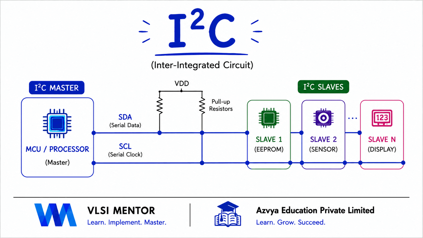
I²C is a two-wire serial bus that connects many devices to one pair of signals: SDA for data and SCL for the clock. Every device hangs off the same two nets, each address is carried in the transfer itself rather than on a dedicated select pin, and no device ever drives a line high — each one can only pull low or let go, with external pull-up resistors restoring the high level. A controller starts and ends every transfer and supplies the clock; a target responds when its address matches. In a chip or board project it is the bus used where cost and pin count matter more than throughput: sensors, EEPROMs, power-management ICs, clock generators, optical-module management, and the sideband register access that configures a larger SoC. It is slow by design and shared by construction, and both of those properties shape how an engineer must reason about it.
Why it exists
Before a shared serial bus, connecting a handful of peripherals meant a parallel bus or a dedicated set of pins per device: address lines, data lines, strobes, and a chip select for each part. Pins are expensive on a package and traces are expensive on a board, and most of those peripherals are configured a few times at boot and then left alone — paying twenty pins for a temperature sensor is paying for bandwidth nobody needs. I²C answers that by spending wires once and distinguishing devices by an address carried in the data stream, so adding a device costs an address rather than a pin. The price is paid elsewhere, and it is worth naming honestly: the bus is slower than a parallel interface, every device shares one failure domain, and because ownership is negotiated rather than assigned, the protocol needs rules for two controllers starting at the same moment.
The part engineers get wrong
Everything that surprises an engineer about I²C follows from one electrical fact: a device can pull a line low or release it, but it can never drive it high. The bus is a wired-AND, and the high level is produced by a resistor. Four consequences follow, and each is a real failure in the field. Rise time is set by that resistor and the bus capacitance, so the maximum clock rate belongs to the board, not to the controller's register. A bit you transmit as 1 that reads back as 0 is not corruption — it is arbitration, and the correct response is to stop driving and retry, not to report an error. A target may hold SCL low to stretch the clock, and the specification places no upper bound on how long, so every timeout in a master is an invention that must be justified rather than a protocol value. And a single device that holds SDA low wedges the whole bus while reporting nothing itself. The same fact is where RTL goes wrong: modelling the pin as a driven logic 1 instead of a release produces a design that simulates perfectly and fails on hardware, because the simulation never had a wired-AND to lose an arbitration on.
Before you start
- Digital logic fundamentals — levels, edges, and reading a timing diagram
- No prior I²C exposure is assumed; the bus is built up from the two wires outward
- For the RTL and verification halves, working Verilog or SystemVerilog and access to a simulator — the protocol is taught, the HDL is assumed
What you will be able to do
- Read an I²C waveform and name every phase: START, address, R/W, ACK, data, repeated START and STOP
- Size a pull-up from bus capacitance and the rise-time budget a given speed mode allows
- Explain why no device drives SDA high, and what that implies for arbitration and for RTL pin modelling
- Choose between a repeated START and a STOP followed by a START, and say what the difference actually costs
- Lay out a board's address map and resolve a collision using strapping, a different part, or a bus switch
- Identify where a target is permitted to stretch the clock, and what a controller must tolerate
- Detect lost arbitration and respond correctly, without misreporting it as a protocol error
- Design an I²C controller and target in RTL, including open-drain pin control, stretching and arbitration
- Build a verification environment with a monitor, a reference model and protocol checks that fire on real violations
- Diagnose a wedged bus, a device that NACKs its address, and a read that returns all ones
- Review an implementation against the timing parameters its speed mode genuinely requires
The learning path
- The bus and its electrical modelWhy I²C exists and what it replaced; open-drain outputs and pull-up sizing; bus architecture and wiring; timing fundamentals
- Framing, addressing and the byteSTART, STOP and repeated START; 7-bit, 10-bit and reserved addressing; the ACK/NACK cycle; write, read and combined transactions
- Timing, stretching and multiple controllersThe named timing parameters and the electrical envelope; clock stretching and its bounds; arbitration and clock synchronisation; speed modes and their limits
- Real devices on a real boardSpecial and reserved protocol features; register-based devices, EEPROMs and sensors, and the addressing patterns they use
- RTL design and implementationController RTL from the command interface to the FSM; target RTL from edge detection to the register interface; FPGA and implementation engineering, including open-drain modelling and synchronisation
- Verification, debugging and reviewVerification architecture and agents; SystemVerilog and UVM environments; assertions, coverage and corner cases; debugging and failure analysis; engineering review and judgment
Core concepts
New to I²C? Work through the curriculum in order — each lesson assumes the one before it, and the sequence is what turns the roadmap above into working knowledge.
Already working with it? Use the core-concept links above to jump straight to the topic you need; each one opens the lesson that covers it in most depth.
Where this leads
Standards: NXP UM10204 — I²C-bus specification and user manual — The bus was defined at Philips and the specification is maintained by NXP; it is the document that fixes the named timing parameters for each speed mode. This track teaches the parameter and what it constrains, and treats a particular device's datasheet number as something to be looked up rather than memorised