
SPI tutorials, labs & MCQs.
An implementation-grade SPI curriculum for RTL design, verification, FPGA and SoC-integration engineers — starting from the full-duplex shift-register model before a single mode table, then SPI timing fundamentals (launch and sample edges, setup/hold, CS lead and lag, slave output valid, round-trip delay), CPOL and CPHA and the four modes derived rather than memorised, device-defined framing, write / read / burst transactions, bus ownership and MISO tri-state contention, performance, datasheet interpretation, SPI flash and boot, Dual / Quad / Octal SPI and XIP, SPI master and slave RTL design, SPI clock domains and FPGA timing constraints, verification planning through monitors, scoreboards, assertions, coverage and UVM, systematic waveform debugging, FPGA / SoC integration, and a design-and-verify capstone.
Tutorials
Learn SPI from beginner to advanced through structured tutorials.
Labs
Practice SPI using progressively challenging hands-on labs.
MCQs
No MCQ papers for SPI yet.
What SPI is
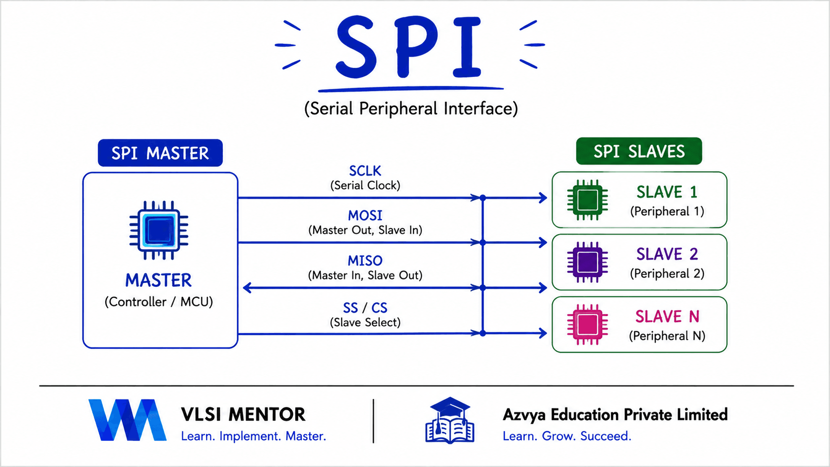
SPI is a clocked, full-duplex serial interface built around a single idea: two shift registers, one in the controller and one in the selected peripheral, wired into a ring and clocked together. The controller drives the clock and a chip-select line, data leaves on one wire and arrives on another, and on every clock edge a bit goes out while a bit comes in. There is no address in the data stream — the controller picks a device by asserting its select — and there is no acknowledgment, no built-in error detection and no formal standard that every part obeys. What a given device expects is defined by its datasheet: which clock polarity and phase, how many command and address bytes, how many idle cycles before read data appears. In a chip or board project SPI is the interface used where throughput matters more than pin count: configuration flash and boot, ADCs and DACs, displays, radios, and sensor parts that would be too slow over a shared two-wire bus.
Why it exists
A shared bus with addressing and arbitration costs something on every transfer: a device must decode an address before it can respond, acknowledgment cycles sit between data bytes, and because no device can drive the line high the maximum clock rate is bounded by a resistor and the board's capacitance. For a boot flash holding tens of megabytes, or an ADC sampling continuously, that overhead is the dominant cost. SPI removes it by spending pins instead: push-pull drivers rather than open-drain, separate wires for each direction so a transfer is a simultaneous exchange rather than a turnaround, and a dedicated select per device so there is nothing to arbitrate and nothing to address. The honest trade is that it scales badly in the other direction — every additional peripheral is another pin and another chip-select trace — and that the absence of a single normative specification moves the specification into each device's datasheet.
The part engineers get wrong
SPI will transfer bits under almost any configuration, which is exactly the problem: nothing on the bus reports that the configuration was wrong. Clock polarity and phase are two independent bits, not four named protocols, and together they decide the one thing that matters — whether an endpoint changes its output on the leading edge and samples on the trailing one, or the reverse. Pick the wrong combination and the link does not fail loudly; it returns data shifted by a bit, or a stream of 0x00 or 0xFF that looks like a dead device rather than a timing error. The same silence covers the rest of the interface. There is no acknowledgment, so a peripheral that was never selected, a MISO line that is disconnected, or a read issued without the dummy cycles the datasheet requires all produce bytes that are indistinguishable from real data at the pins. Debugging SPI therefore starts from the datasheet and the waveform rather than from the data, and the question to ask of a working link is not whether bytes arrive but whether both ends agree on which edge owns them.
Before you start
- Digital logic fundamentals — clocks, edges, shift registers and reading a timing diagram
- No prior SPI exposure is assumed; the interface is built up from the shift-register model outward
- For the RTL and verification halves, working Verilog or SystemVerilog and access to a simulator
What you will be able to do
- Describe any SPI transfer as two shift registers exchanging contents, and predict what each end receives
- Derive a mode's sampling and shifting behaviour from CPOL and CPHA instead of recalling four tables
- Recognise the waveform signature of a mode mismatch, and distinguish it from a dead or unselected device
- Read a device datasheet and turn it into a transaction specification: command, address, dummy cycles, data
- Extract setup, hold and maximum clock figures from a datasheet and check a proposed clock rate against them
- Choose between one chip select per device and a daisy chain, and state the cost of each
- Explain why a read is a write of don't-care bytes, and why read latency lives in the protocol rather than the wire
- Design an SPI controller and peripheral in RTL, including edge control, shift registers and chip-select generation
- Cross an SPI interface into a different clock domain without sampling a bit twice or missing one
- Verify sampling and shifting behaviour with assertions and coverage over all four modes
- Debug a link that returns all ones, all zeros, or data off by a single bit
The learning path
- The model and its timingWhy SPI exists; signal ownership; the shift-register mental model; full-duplex exchange; bus topologies; timing fundamentals
- CPOL, CPHA and the four modesClock polarity and phase as independent choices; deriving behaviour rather than memorising it; each of the four modes; the failure signature of a mismatch
- TransactionsFraming; write transactions; read transactions, dummy phases and latency; multi-byte, burst and continuous transfers
- Systems, devices and performanceBus ownership and multi-peripheral systems; throughput and clocking; reading real datasheets; SPI flash and boot; dual, quad and octal SPI, and execute-in-place
- RTL designDesigning a controller in RTL; designing a peripheral in RTL; clock domains and FPGA timing closure
- Verification, debugging and integrationVerification fundamentals; assertions, coverage and UVM; debugging and waveform reasoning; FPGA and SoC integration; a capstone configurable controller designed and verified end to end
Core concepts
New to SPI? Work through the curriculum in order — each lesson assumes the one before it, and the sequence is what turns the roadmap above into working knowledge.
Already working with it? Use the core-concept links above to jump straight to the topic you need; each one opens the lesson that covers it in most depth.
Where this leads
Standards: Device datasheets, and de-facto industry conventions — SPI has no governing standard body: there is no IEEE or ISO document defining it, and the four-mode naming is a widely shared convention rather than a normative requirement. Each device's datasheet is the specification for that device, which is why this track teaches datasheet reading as a protocol skill rather than an appendix