
DDR tutorials, labs & MCQs.
The most complete DDR curriculum on the internet — starting from the memory hierarchy and the memory-wall problem before touching a single DDR signal, then through DRAM fundamentals (1T1C cell, destructive read, refresh), the DDR generation evolution (SDR / DDR1..5 / LPDDR / HBM), DDR architecture and signals, commands and addressing, activate / precharge, reads / writes / bursts, the full timing-parameter family (tRCD / tRP / tRAS / tRC / tWR / tCCD / tRRD / tFAW / CL / CWL), refresh, banks and bank groups, the DDR controller (scheduler / command queue / refresh / arbitration), address mapping, the DDR PHY, DQS and data capture, training, ODT and SI, performance, LPDDR, DDR5, HBM, verification, debugging, SoC integration, real-industry case studies (CPU / GPU / mobile / AI / data centre), pre-tapeout review checklists, and the misconceptions section.
Tutorials
Learn DDR from beginner to advanced through structured tutorials.
Labs
Practice DDR using progressively challenging hands-on labs.
MCQs
No MCQ papers for DDR yet.
What DDR is
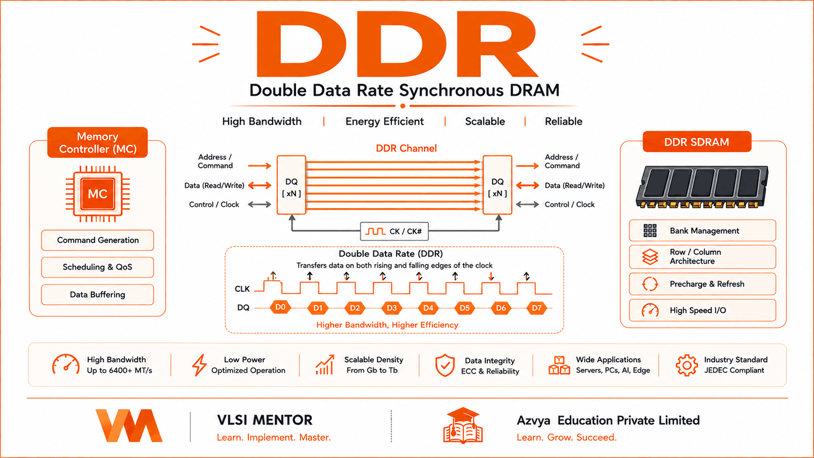
DDR is the interface discipline that lets a processor use DRAM as its working memory. The device itself stores each bit as charge on a tiny capacitor reached through one transistor, which is why DRAM is dense and cheap per bit — and why it must be refreshed, why reading a row is a destructive operation the device has to undo, and why an access is a sequence of commands rather than a single addressed read. DDR is the agreement that organises all of that: a command and address bus, a data bus clocked on both edges of a differential clock, a set of timing parameters the controller must never violate, and a device organised into banks, bank groups and ranks so several operations can be in flight at once. For an engineer, the subject is really three blocks — the memory controller that schedules commands, the PHY that gets data across the physical channel with usable timing margin, and the DRAM device whose rules both must respect.
Why it exists
A cache miss has to be served from somewhere, and no practical technology gives capacity, low latency and low cost per bit at the same time. DRAM is the answer the industry settled on for the working-memory tier, so the interface to it sits directly under the performance of everything above: a core stalled on a load, a DMA engine streaming a frame, an accelerator whose arithmetic units are only as busy as their operand supply. What makes DDR an engineering discipline rather than a wiring standard is that the device imposes constraints — a row must be opened before a column can be read, a bank must be closed before a different row can be opened, refresh must happen whether the system is busy or not — and the order in which a controller resolves those constraints decides how much of the interface's nominal bandwidth a real workload ever sees.
The part engineers get wrong
The most useful habit to build early is refusing to treat DDR latency as a single number. An access is a sequence of commands whose cost depends on the state the target bank is already in: the same physical device answers a request quickly when the needed row is already open and much more slowly when a different row has to be closed and opened first. That state is a consequence of the access pattern and of the controller's own scheduling and address-mapping policy, which means observed memory latency is a property of the system rather than a specification of the part. The second thing worth holding is where the boundaries sit: command scheduling and address mapping are controller work, data capture and timing margin are PHY work, and the retention and timing rules both must obey belong to the device. Most DDR questions resolve as soon as you decide which of those three owns the behaviour in front of you.
Before you start
- Digital design — synchronous logic, state machines and clock domains
- Basic computer architecture: what a cache is and what happens on a miss
- Helpful but not required: any prior exposure to an on-chip bus such as AXI
What you will be able to do
- Explain why a memory hierarchy exists, and which tier DDR occupies in it
- Reason about a DRAM access as a command sequence rather than a single latency figure
- Read a DDR timing parameter and say which physical constraint it encodes
- Separate controller responsibilities from PHY responsibilities when reasoning about a failure
- Explain how address mapping and scheduling policy change a workload's achieved bandwidth
- Discuss the DDR4 to DDR5 changes in terms of the problems they were introduced to solve
The learning path
- Why DRAM existsThe memory hierarchy, the technology trade space, and the memory-wall problem
- DRAM fundamentalsThe 1T1C cell, leakage and refresh, destructive read and restore
- Array and device architectureRows, columns, sense amplifiers, banks, bank groups, ranks and channels
- Signals, commands and addressingThe wire-level vocabulary and how an address becomes row, column and bank
- Access sequencesActivate and precharge, reads, writes, bursts, and the row buffer
- TimingWhere each timing parameter comes from and how it constrains scheduling
- The controllerCommand scheduling, queues, refresh management, arbitration and address mapping
- The PHY and trainingSerialisation, DQS-based capture, leveling and calibration
- Generations, verification and debugDDR5, LPDDR and HBM, compliance verification, and silicon bring-up debug
Core concepts
New to DDR? Work through the curriculum in order — each lesson assumes the one before it, and the sequence is what turns the roadmap above into working knowledge.
Already working with it? Use the core-concept links above to jump straight to the topic you need; each one opens the lesson that covers it in most depth.
Where this leads
Standards: JEDEC — Publishes the JESD79 DDR SDRAM standards and the LPDDR specifications